ICS9DB104 Overview
Description
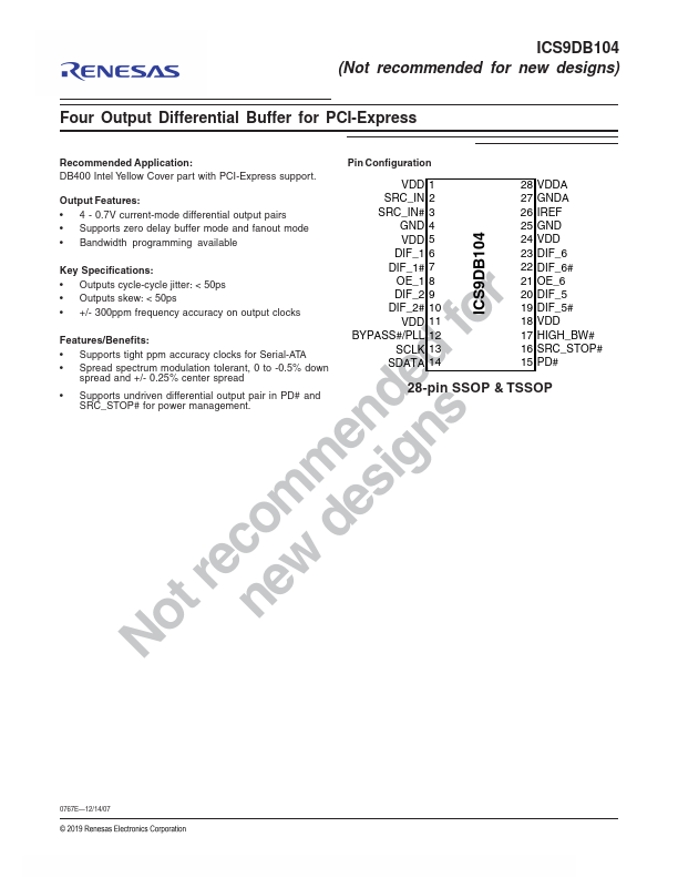
PWR IN IN PWR PWR OUT OUT IN OUT OUT PWR IN IN I/O Power supply, nominal 3.3V 0.7 V Differential SRC TRUE input 0.7 V Differential SRC COMPLEMENTARY input Ground pin. Power supply, nominal 3.3V 0.7V differential true clock outputs 0.7V differential complement clock outputs Active high input for enabling outputs.
Key Features
- 4 - 0.7V current-mode differential output pairs
- Supports zero delay buffer mode and fanout mode
- Bandwidth programming available SRC_IN 2 SRC_IN# 3 GND 4 VDD 5 DIF_1 6 27 GNDA 26 IREF 25 GND 24 VDD 23 DIF_6 ICS9DB104 Key Specifications
- Outputs cycle-cycle jitter: < 50ps
- Outputs skew: < 50ps r
- +/- 300ppm frequency accuracy on output clocks foFeatures/Benefits
- Supports tight ppm accuracy clocks for Serial-ATA d
- Spread spectrum modulation tolerant, 0 to -0.5% down spread and +/- 0.25% center spread e