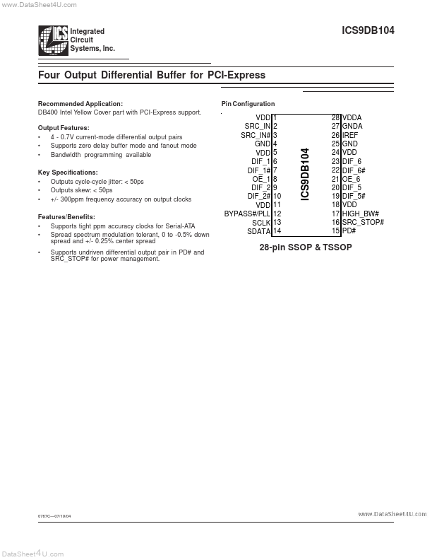
• Part: ICS9DB104
  • Manufacturer: Integrated Circuit Systems
  • Size: 263.73 KB
Download ICS9DB104 Datasheet PDF
ICS9DB104 page 2
Page 2
ICS9DB104 page 3
Page 3

ICS9DB104 Description

Power supply, nominal 3.3V 0.7V differential true clock outputs 0.7V differential plement clock outputs Active high input for enabling outputs. 0 = tri-state outputs, 1= enable outputs 0.7V differential true clock outputs 0.7V differential plement clock outputs Power supply, nominal 3.3V Input to select Bypass(fan-out) or PLL (ZDB) mode 0 = Bypass mode, 1= PLL mode Clock pin of SMBus circuitry, 5V tolerant. Data pin...

ICS9DB104 Key Features

  • 0.7V current-mode differential output pairs
  • Supports zero delay buffer mode and fanout mode
  • Bandwidth programming available Key Specifications
  • Outputs cycle-cycle jitter: < 50ps
  • Outputs skew: < 50ps
  • +/- 300ppm frequency accuracy on output clocks Features/Benefits
  • Supports tight ppm accuracy clocks for Serial-ATA
  • Spread spectrum modulation tolerant, 0 to -0.5% down spread and +/- 0.25% center spread
  • Supports undriven differential output pair in PD# and SRC_STOP# for power management