Datasheet4U Logo Datasheet4U.com

ICS9DB108 - Eight Output Differential Buffer

Description

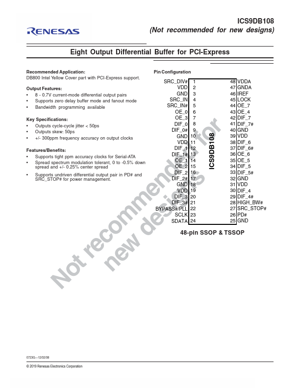
PIN # PIN NAME 1 SRC_DIV# 2 VDD 3 GND 4 SRC_IN 5 SRC_IN# 6 OE_0 7 OE_3 8 DIF_0 9 DIF_0# 10 GND 11 VDD 12 DIF_1 13 DIF_1# 14 OE_1 15 OE_2 16 DIF_2 17 DIF_2# 18 GND 19 VDD 20 DIF_3 21 DIF_3# 22 BYPASS#/PLL 23 SCLK 24 SDATA PIN TYPE DESCRIPTION IN PWR PWR IN IN IN IN OUT OUT PWR PWR OUT OUT IN IN OU

Features

  • 8 - 0.7V current-mode differential output pairs.
  • Supports zero delay buffer mode and fanout mode.
  • Bandwidth programming available VDD GND SRC_IN SRC_IN# OE_0 2 3 4 5 6 47 GNDA 46 IREF 45 LOCK 44 OE_7 43 OE_4 Key Specifications:.
  • Outputs cycle-cycle jitter < 50ps r.
  • Outputs skew: 50ps.
  • +/- 300ppm frequency accuracy on output clocks foFeatures/Benefits:.
  • Supports tight ppm accuracy clocks for Serial-ATA d.
  • Spread spectrum.

📥 Download Datasheet

Datasheet preview – ICS9DB108

Datasheet Details

Part number ICS9DB108
Manufacturer Renesas
File Size 300.19 KB
Description Eight Output Differential Buffer
Datasheet download datasheet ICS9DB108 Datasheet
Additional preview pages of the ICS9DB108 datasheet.
Other Datasheets by Renesas

Full PDF Text Transcription

Click to expand full text
Integrated Circuit Systems, Inc. ICS9DB108 (Not recommended for new designs) Eight Output Differential Buffer for PCI-Express Recommended Application: Pin Configuration DB800 Intel Yellow Cover part with PCI-Express support. SRC_DIV# 1 48 VDDA Output Features: • 8 - 0.7V current-mode differential output pairs • Supports zero delay buffer mode and fanout mode • Bandwidth programming available VDD GND SRC_IN SRC_IN# OE_0 2 3 4 5 6 47 GNDA 46 IREF 45 LOCK 44 OE_7 43 OE_4 Key Specifications: • Outputs cycle-cycle jitter < 50ps r• Outputs skew: 50ps • +/- 300ppm frequency accuracy on output clocks foFeatures/Benefits: • Supports tight ppm accuracy clocks for Serial-ATA d• Spread spectrum modulation tolerant, 0 to -0.5% down spread and +/- 0.
Published: |