ICS9DB102
Overview
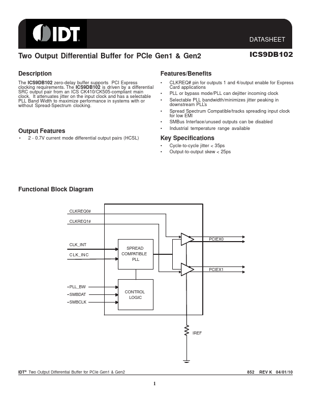
The ICS9DB102 zero-delay buffer supports PCI Express clocking requirements. The ICS9DB102 is driven by a differential SRC output pair from an ICS CK410/CK505-compliant main clock.
- 2 - 0.7V current mode differential output pairs (HCSL) Features/Benefits
- CLKREQ# pin for outputs 1 and 4/output enable for Express Card applications
- PLL or bypass mode/PLL can dejitter incoming clock
- Selectable PLL bandwidth/minimizes jitter peaking in downstream PLL’s
- Spread Spectrum Compatible/tracks spreading input clock for low EMI
- SMBus Interface/unused outputs can be disabled
- Industrial temperature range available Key Specifications
- Cycle-to-cycle jitter < 35ps
- Output-to-output skew < 25ps Functional Block Diagram