ICS9DB102
Overview
- 2 - 0.7V current mode differential output pairs (HSCL) Key Specifications:
- Cycle-to-cycle jitter < 35ps
- Output-to-output skew < 25 ps Features/Benefits:
- CLKREQ# pin for outputs 1 and 4/output enable for Express Card applications
- PLL or bypass mode/PLL can dejitter incoming clock
- Selectable PLL bandwidth/minimizes jitter peaking in downstream PLL’s
- Spread Spectrum Compatible/tracks spreading input clock for low EMI
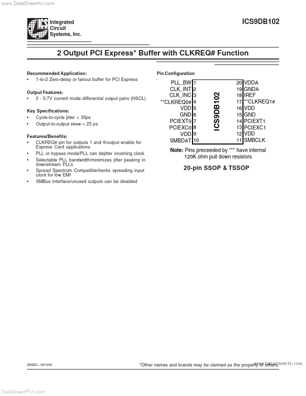
- SMBus Interface/unused outputs can be disabled Pin Configuration PLL_BW CLK_INT CLK_INC **CLKREQ0# VDD GND PCIEXT0 PCIEXC0 VDD SMBDAT