Datasheet4U.com
🌙
M6MGB33BS8AWG-P
M6MGB33BS8BWG-P
M6MGB33BS8BWG
M6MGB331S4BKT
M6MGB331S8BKT
M6MGB331S8AKT
M6MGB33BS8AWG-P Datasheet | Renesas
Part:
M6MGB33BS8AWG-P
Description:
CMOS SRAM
Manufacturer:
Renesas
Size:
160.61 KB
M6MGB33BS8AWG-P Datasheet (PDF) Download
Renesas
M6MGB33BS8AWG-P
Description
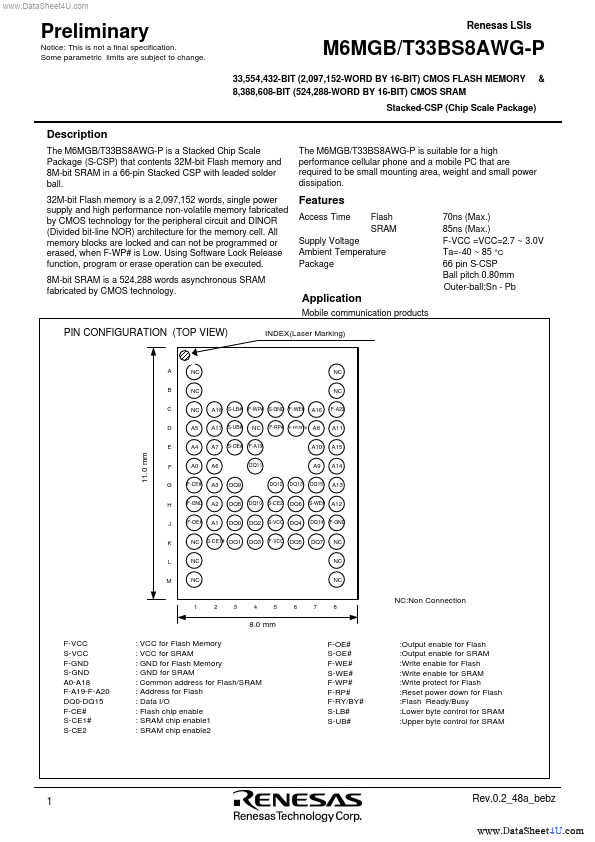
The M6MGB/T33BS8AWG-P is a Stacked Chip Scale Package (S-CSP) that.
×
Close