RC21012A
RC21012A is manufactured by Renesas.
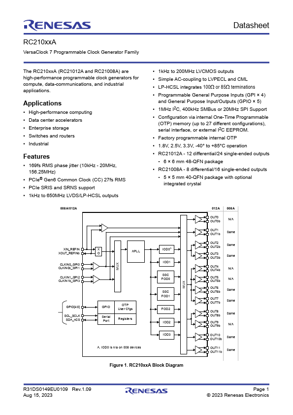
RC210xxA
VersaClock 7 Programmable Clock Generator Family
The RC210xxA (RC21012A and RC21008A) are high-performance programmable clock generators for pute, data-munications, and industrial applications.
Applications
- High-performance puting
- Data center accelerators
- Enterprise storage
- Switches and routers
- Industrial
Features
- 169fs RMS phase jitter (10kHz
- 20MHz, 156.25MHz)
- PCIe® Gen6 mon Clock (CC) 27fs RMS
- PCIe SRIS and SRNS support
- 1kHz to 650MHz LVDS/LP-HCSL outputs
008 A/012A
XIN_REFIN
XOUT_REFINb
CLKIN0_GPI0 CLKIN0b_GPI1
CLKIN1_GPI2 CLKIN1b_GPI3
APL L
GPIO[4:0]
SCL_SCLK SDA_nCS
GPIO
Ser ial Por t
OTP Use r Cfgs
Registe rs
A. IOD0...