SLG74190
SLG74190 is 1 to 19 Differential Clock Buffer manufactured by Renesas.
Features
- Intel DB1900Z Clock Specification Revision 1.0
- 1:19 Differential Zero Delay Buffer
- PCIe Gen 2/Gen3 & Intel ® QPI
- 100ps Input to Output Delay
- HCSL Output Buffer
- Configuration PLL (ZDB) and Bypass Mode
- Programmable PLL Bandwidth
- 72 pin QFN package (6/6 Ro HS pliant)
1 to 19 Differential Clock Buffer
Output Summary
- 19
- differential clock output pairs @ 0.7V
- 8
- OE# input pins to control output
- 1
- differential external feedback output pair
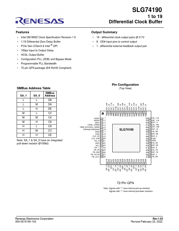
SMBus Address Table
SA_1 L L L M M M H H H
SA_0 L M H L M H L M H
SMBus Address
D8 DA DE C2 C4 C6 CA CC CE
Note: SA_1 & SA_0 have an integrated pull-down resistor @100kΩ
Pin Configuration
(Top View)
72 DIF_18# 71 DIF_18 70 DIF_17# 69 DIF_17 68 VDD 67 DIF_16# 66 DIF_16 65 DIF_15# 64 DIF_15 63 GND 62 DIF_14# 61 DIF_14 60 DIF_13# 59 DIF_13 58 VDD 57 OE_12# 56 DIF_12# 55 DIF_12
VDDA
GNDA
IREF
- 100M_133M#
HBW_BYPASS_LBW#
PWRGD/PWRDN#
CLK_IN...