Datasheet4U Logo Datasheet4U.com

UPA2763 - MOS FIELD EFFECT TRANSISTOR

General Description

The μ PA2763 is N-channel MOS Field Effect Transistor designed for DC/DC converter and power management applications.

Key Features

  • Low on-state resistance ⎯ RDS(on)1 = 23.0 mΩ MAX. (VGS = 10 V, ID = 21 A) ⎯ RDS(on)2 = 28.0 mΩ MAX. (VGS = 8 V, ID = 21 A).
  • Low Ciss 2100 pF TYP.
  • Built-in gate protection diode.
  • Thin type surface mount package with heat spreader (8-pin HVSON).
  • RoHS Compliant Absolute Maximum Ratings (TA = 25°C) Item Drain to Source Voltage (VGS = 0 V) Gate to Source Voltage (VDS = 0 V) Drain Current (DC) (TC = 25°C) Drain Current (pulse) ∗1 Total Power Dissipation∗.

📥 Download Datasheet

Datasheet Details

Part number UPA2763
Manufacturer Renesas
File Size 260.35 KB
Description MOS FIELD EFFECT TRANSISTOR
Datasheet download datasheet UPA2763 Datasheet

Full PDF Text Transcription for UPA2763 (Reference)

Note: Below is a high-fidelity text extraction (approx. 800 characters) for UPA2763. For precise diagrams, and layout, please refer to the original PDF.

Preliminary Data Sheet μ PA2763 MOS FIELD EFFECT TRANSISTOR Description 
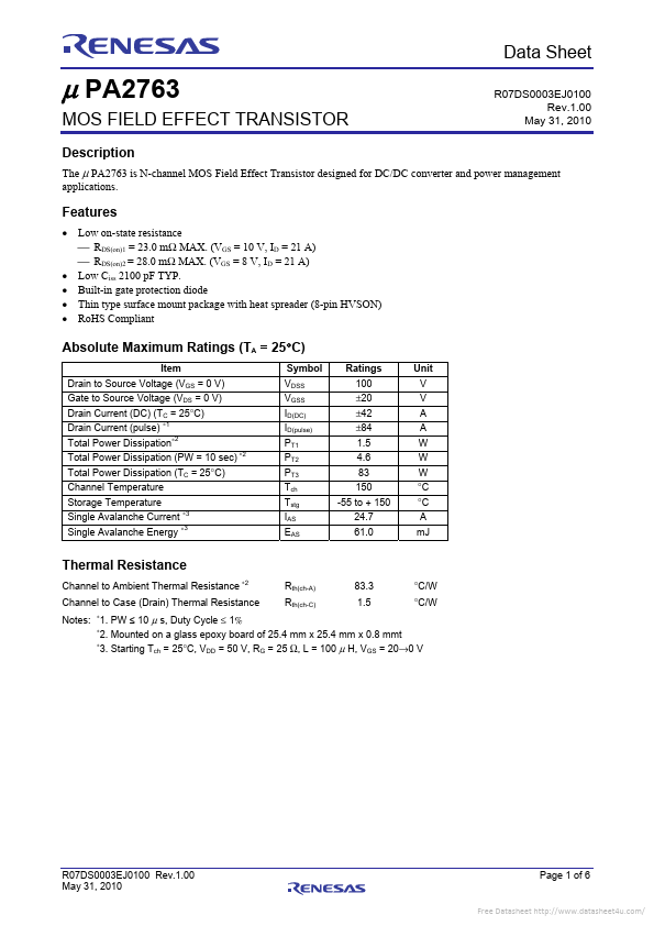
R07DS0003EJ0100 Rev.1.00 May 31, 2010 The μ PA2763 is N-channel MOS Field Effect Transistor design...

View more extracted text
31, 2010 The μ PA2763 is N-channel MOS Field Effect Transistor designed for DC/DC converter and power management applications. Features • Low on-state resistance ⎯ RDS(on)1 = 23.0 mΩ MAX. (VGS = 10 V, ID = 21 A) ⎯ RDS(on)2 = 28.0 mΩ MAX. (VGS = 8 V, ID = 21 A) • Low Ciss 2100 pF TYP.