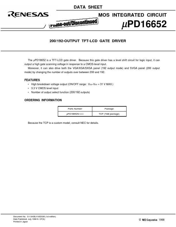
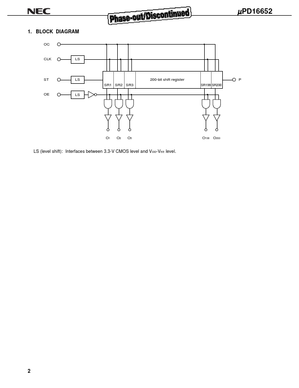
Symbol O1 to O200
ST P
CLK OE OC
VDD VCC VSS
Pin Name Driver output pins
Start pulse input pin Cascade output pin
Shift clock input Enable input Input to select number of outputs
Positive power supply for driver Reference power supply Ground
Description
Scan signal output pins that drive the gate
Key Features
High breakdown voltage output (ON/OFF range: VDD-VEE = 31 V MAX. ).
3.3 V CMOS level input.
Number of output select function (200/192 outputs).
Full PDF Text Transcription for uPD16652 (Reference)
Note: Below is a high-fidelity text extraction (approx. 800 characters) for
uPD16652. For precise diagrams, and layout, please refer to the original PDF.
DATA SHEET MOS INTEGRATED CIRCUIT µPD16652 200/192-OUTPUT TFT-LCD GATE DRIVER The µPD16652 is a TFT-LCD gate driver. Because this gate driver has a level shift circuit fo...
View more extracted text
LCD gate driver. Because this gate driver has a level shift circuit for logic input, it can output a high gate scanning voltage in response to a CMOS-level input. Moreover, it can also drive both the VGA/XGA/SXGA panel (192 output mode) and SVGA panel (200 output mode) by changing the number of outputs over between 200 and 192. FEATURES • High breakdown voltage output (ON/OFF range: VDD-VEE = 31 V MAX.) • 3.3 V CMOS level input • Number of output select function (200/192 outputs) ORDERING INFORMATION Parts Number µPD16652N-××× Package TCP (TAB package) Because the TCP is a custom model, consult NEC for details. Document No