DESCRIPTION
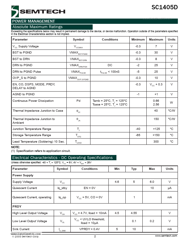
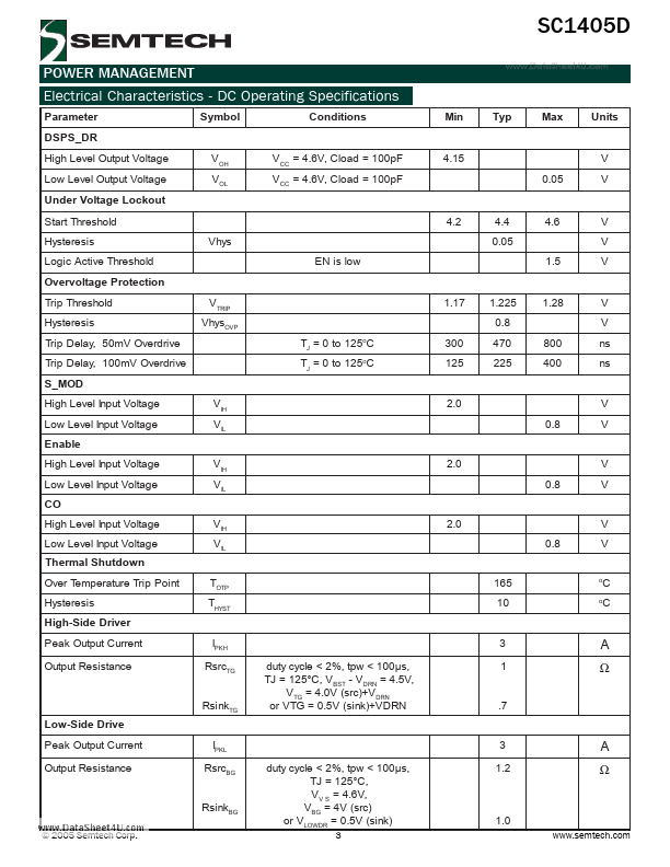
Adaptive Overlap Protection circuit ensures that the synchronous FET does not turn on until the top FET source has reached a voltage low enough to prevent shoot-through. The bottom FET may be disabled at light loads by keeping S_MOD low to trigger asynchronous operation, thus saving the bottom FET’s gate drive current and inductor ripple current. An internal voltage reference allows threshold adjustment for an Output Over-Voltage protection circuitry, independent of the PWM controller. The device provides overvoltage protection independent of the PWM feedback loop with a unique “adaptive OVP” comparator which rejects noise but responds quickly to a true OVP situation. Under-Voltage-Lock-Out circuit is included to guarantee that both driver outputs are off when Vcc is less than or equal to 4.4V (typ) at supply ramp up (4.35V at supply ramp down). A CMOS output provides status indication of the 5V supply. A low enable input places the IC in standby mode, reducing supply current to less than 10µA. Semtech Corporation