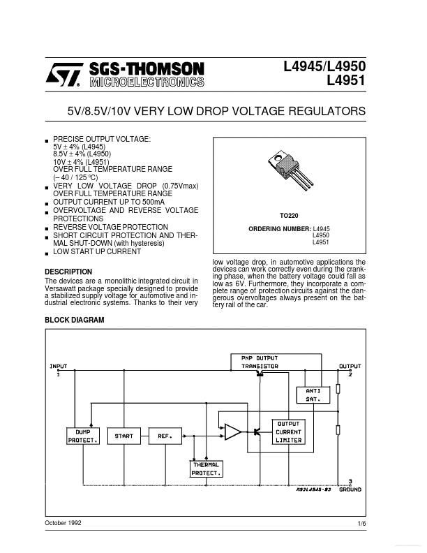
DESCRIPTION
Thanks to their very BLOCK DIAGRAM TO220 ORDERING NUMBER: L4945 L4950 L4951 low voltage drop, in automotive applications the devices can work correctly even during the cranking phase, when the battery voltage could fall as low as 6V. Furthermore, they incorporate a complete range of protection circuits against the dangerous overvoltages always present on the battery rail of the car. Details are subject to change without notice. October 1992 1/6 Free Datasheet L4945 - L4950 - L4951 ABSOLUTE MAXIMUM RATINGS
Symbol Vi Parameter DC Input Voltage DC Reverse Input Voltage Transient Input Overvoltages : Load Dump : 5ms ≤ trise ≤ 10ms τf Fall Time Constant = 100ms RSOURCE ≥ 0.5Ω Field Decay : 5ms ≤ tfall ≤ 10ms, RSOURCE ≥ 10Ω τr Rise Time Constant = 33ms Low Energy Spike : trise = 1µs, tfall = 500µs, R SOURCE ≥ 10Ω fr Repetition Frequency = 5Hz Junction Temperature Range Operating Temperature Range Storage Temperature Range Value 35 – 18 80 Unit V V V – 80 ± 100 V V TJ TOP Tstg – 40 to 150 – 40 to 125 – 55 to 150 °C °C °C Note: The circuit is ESD protected according to MIL-STD-883C. SGS-THOMSON