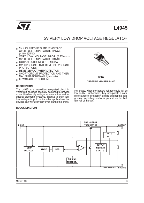
DESCRIPTION
Thanks to their very low voltage drop, in automotive applications the devices can work correctly even during the crankBLOCK DIAGRAM TO220 ORDERING NUMBER: L4945 ing phase, when the battery voltage could fall as low as 6V. Furthermore, they incorporate a complete range of protection circuits against the dangerous overvoltages always present on the battery rail of the car. Details are subject to change without notice. March 1999 1/6 L4945 ABSOLUTE MAXIMUM RATINGS
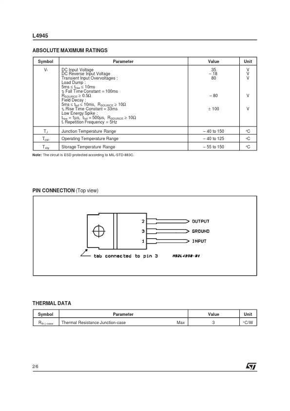
Symbol Vi Parameter DC Input Voltage DC Reverse Input Voltage Transient Input Overvoltages : Load Dump : 5ms ≤ trise ≤ 10ms τf Fall Time Constant = 100ms RSOURCE ≥ 0.5Ω Field Decay : 5ms ≤ tfall ≤ 10ms, RSOURCE ≥ 10Ω τr Rise Time Constant = 33ms Low Energy Spike : trise = 1µs, tfall = 500µs, RSOURCE ≥ 10Ω fr Repetition Frequency = 5Hz Junction Temperature Range Operating Temperature Range Storage Temperature Range Value 35 – 18 80 Unit V V V – 80 ± 100 V V TJ TOP Tstg – 40 to 150 – 40 to 125 – 55 to 150 °C °C °C Note: The circuit is ESD protected according to MIL-STD-883C. STMicroelectronics