M29F002NT
M29F002NT is 2 Mbit 256Kb x8 / Boot Block Single Supply Flash Memory manufactured by STMicroelectronics.
M29F002T, M29F002NT M29F002B
2 Mbit (256Kb x8, Boot Block) Single Supply Flash Memory
5V ± 10% SUPPLY VOLTAGE for PROGRAM, ERASE and READ OPERATIONS FAST ACCESS TIME: 70ns FAST PROGRAMMING TIME: 10µs typical PROGRAM/ERASE CONTROLLER (P/E.C.)
- Program Byte-by-Byte
- Status Register bits MEMORY BLOCKS
- Boot Block (Top or Bottom location)
- Parameter and Main blocks BLOCK, MULTI-BLOCK and CHIP ERASE MULTI-BLOCK PROTECTION/TEMPORARY UNPROTECTION MODES ERASE SUSPEND and RESUME MODES
- Read and Program another Block during Erase Suspend LOW POWER CONSUMPTION
- Stand-by and Automatic Stand-by 100,000 PROGRAM/ERASE CYCLES per BLOCK 20 YEARS DATA RETENTION
- Defectivity below 1ppm/year ELECTRONIC SIGNATURE
- Manufacturer Code: 20h
- Device Code, M29F002T: B0h
- Device Code, M29F002NT: B0h
- Device Code, M29F002B: 34h DESCRIPTION The M29F002 is a non-volatile memory that may be erased electrically at the block or chip level and programmed in-system on a Byte-by-Byte basis using only a single5V VCC supply.For Program and Erase operations the necessary high voltages are generated internally. The device can also be programmed in standard programmers. The array matrix organisation allows each block to be erased and reprogrammed without affecting other blocks. Blocks can be protected against programing and erase on programming equipment, and temporarily unprotected to make changes in the application. Each block can be programmed and erased over 100,000 cycles.
July 1998
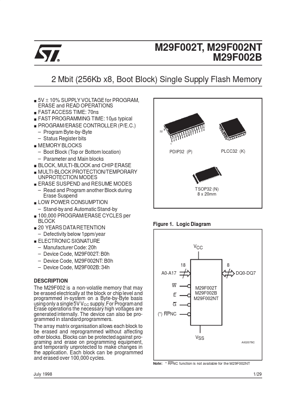
PDIP32 (P)
PLCC32 (K)
TSOP32 (N) 8 x 20mm
Figure 1. Logic Diagram
18 A0-A17 W E G (- ) RPNC M29F002T M29F002B M29F002NT
8 DQ0-DQ7
AI02078C
Note:
- RPNC function is not available for the M29F002NT
1/29
M29F002T, M29F002NT, M29F002B
Figure 2A. DIP Pin Connections Figure 2B. LCC Pin Connections
(- ) RPNC A16 A15 A12 A7 A6 A5 A4 A3 A2 A1 A0 DQ0 DQ1 DQ2 VSS
DQ1 DQ2 VSS DQ3 DQ4 DQ5...