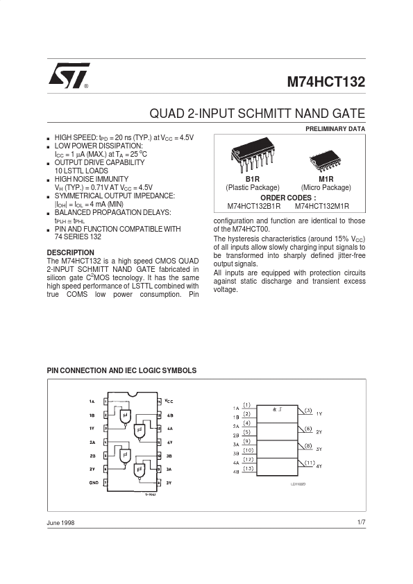
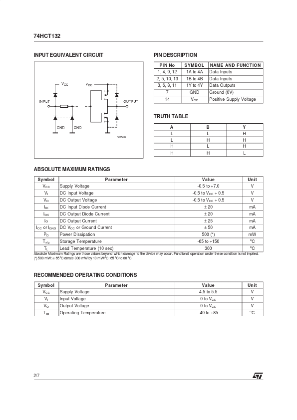
Datasheet4U Logo Datasheet4U.com

M74HCT132 Datasheet Quad 2-input Schmitt Nand Gate

Manufacturer: STMicroelectronics

Overview: ® M74HCT132 QUAD 2-INPUT SCHMITT NAND GATE PRELIMINARY DATA s s s s s s s HIGH SPEED: tPD = 20 ns (TYP.) at VCC = 4.5V LOW POWER DISSIPATION: ICC = 1 µA (MAX.) at TA = 25 oC OUTPUT DRIVE CAPABILITY 10 LSTTL LOADS HIGH NOISE IMMUNITY VH (TYP.) = 0.71V AT VCC = 4.5V SYMMETRICAL OUTPUT IMPEDANCE: |IOH| = IOL = 4 mA (MIN) BALANCED PROPAGATION DELAYS: tPLH ≅ tPHL PIN AND FUNCTION PATIBLE WITH 74 SERIES 132 B1R M1R (Plastic Package) (Micro Package) ORDER CODES : M74HCT132B1R M74HCT132M1R configuration and function are identical to those of the M74HCT00. The hysteresis characteristics (around 15% VCC) of all inputs allow slowly charging input signals to be transformed into sharply defined jitter-free output signals. All inputs are equipped with protection circuits against static discharge and transient excess voltage.

General Description

The M74HCT132 is a high speed CMOS QUAD 2-INPUT SCHMITT NAND GATE fabricated in silicon gate C2MOS tecnology.

It has the same high speed performance of LSTTL bined with true S low power consumption.

Pin PIN CONNECTION AND IEC LOGIC SYMBOLS June 1998 1/7 74HCT132 INPUT EQUIVALENT CIRCUIT PIN DESCRIPTION PIN No 1, 4, 9, 12 2, 5, 10, 13 3, 6, 8, 11 7 14 SYMBOL 1A to 4A 1B to 4B 1Y to 4Y GND VCC NAME AND F UNCTIO N Data Inputs Data Inputs Data Outputs Ground (0V) Positive Supply Voltage TRUTH TABLE A L L H H B L H L H Y H H H L ABSOLUTE MAXIMUM RATINGS Symbol VCC VI VO IIK IOK IO PD Tstg TL Supply Voltage DC Input Voltage DC Output Voltage DC Input Diode Current DC Output Diode Current DC Output Current Power Dissipation Storage Temperature Lead Temperature (10 sec) Parameter Value -0.5 to +7.0 -0.5 to VCC + 0.5 -0.5 to VCC + 0.5 ± 20 ± 20 ± 25 ± 50 500 (*) -65 to +150 300 Unit V V V mA mA mA mA mW o o ICC or IGND DC VCC or Ground Current C C Absolute Maximum Ratings are those values beyond which damage to the device may occur.

M74HCT132 Distributor