STB13005 Overview
Key Specifications
Package: TO-262-3
Mount Type: Through Hole
Pins: 3
Max Operating Temp: 150 °C
Description
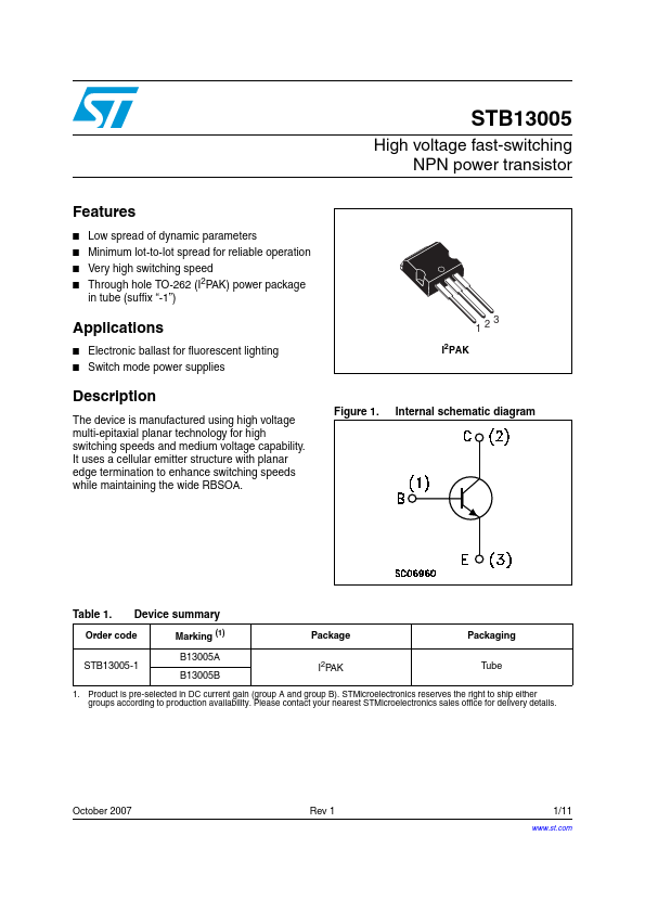
The device is manufactured using high voltage multi-epitaxial planar technology for high switching speeds and medium voltage capability. It uses a cellular emitter structure with planar edge termination to enhance switching speeds while maintaining the wide RBSOA.
Key Features
- Low spread of dynamic parameters
- Minimum lot-to-lot spread for reliable operation
- Very high switching speed
- Through hole TO-262 (I2PAK) power package in tube (suffix “-1”)