• Part: STB160NF02L
  • Description: N-CHANNEL POWER MOSFET
  • Category: MOSFET
  • Manufacturer: STMicroelectronics
  • Size: 274.94 KB
Download STB160NF02L Datasheet PDF
STMicroelectronics
STB160NF02L
STB160NF02L is N-CHANNEL POWER MOSFET manufactured by STMicroelectronics.
ION 
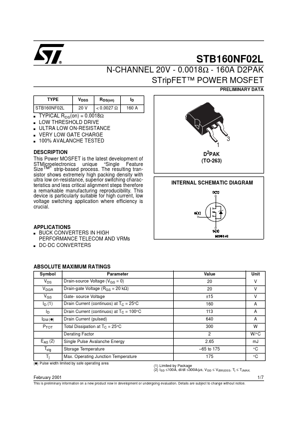
This Power MOSFET is the latest development of STMicroelectronics unique “Single Feature Size™” strip-based process. The resulting transistor shows extremely high packing density with ultra low on-resistance, superior switching characteristics and less critical alignment steps therefore a remarkable manufacturing reproducibility. This device is particularly suitable for high current, low voltage switching application where efficiency is crucial. INTERNAL SCHEMATIC DIAGRAM APPLICATIONS s BUCK CONVERTERS IN HIGH PERFORMANCE TELE AND VRMs s DC-DC CONVERTERS ABSOLUTE MAXIMUM RATINGS Symbol VDS VDGR VGS ID (1) ID IDM (q) PTOT EAS (2) Tstg Tj Parameter Drain-source Voltage (VGS = 0) Drain-gate Voltage (RGS = 20 kΩ) Gate- source Voltage Drain Current (continuos) at TC = 25°C Drain Current (continuos) at TC = 100°C Drain Current (pulsed) Total Dissipation at TC = 25°C Derating Factor Single Pulse Avalanche Energy Storage Temperature Max. Operating Junction Temperature Value 20 20 ±15 160 113 640 300 2 2.65 - 65 to 175 175 (1) Limited by Package (2) I SD ≤100A, di/dt ≤300A/µs, V DD ≤ V(BR)DSS, Tj ≤ TJMAX. Unit V V V A A A W W/°C m J °C °C (q) Pulse width limited by safe operating area February 2001 This is preliminary information on a new product now in development or undergoing evaluation. Details are subject to change without notice. 1/7 THERMAL DATA Rthj-case Rthj-amb Tl Thermal Resistance Junction-case Max Thermal Resistance Junction-ambient Max Maximum Lead Temperature For Soldering Purpose 0.5 62.5 300 °C/W °C/W °C ELECTRICAL CHARACTERISTICS (TCASE = 25 °C UNLESS OTHERWISE SPECIFIED) OFF Symbol V(BR)DSS IDSS IGSS Parameter Drain-source Breakdown Voltage Zero Gate Voltage Drain Current (VGS = 0) Gate-body Leakage Current (VDS = 0) Test Conditions ID = 250 µA, VGS = 0 VDS = Max Rating VDS = Max Rating, TC = 125 °C VGS = ±15V Min. 20 1 10 ±100 Typ. Max. Unit V µA µA n A ON (1) Symbol VGS(th) RDS(on) ID(on) Parameter Gate Threshold Voltage Static...