Download STB16PF06L Datasheet PDF
STMicroelectronics
STB16PF06L
STB16PF06L is P-CHANNEL MOSFET manufactured by STMicroelectronics.
ures TYPE STB16PF06L s s s Figure 1: Package ID 16 A Pw 70 W VDSS 60 V RDS(on) < 0.125 Ω TYPICAL RDS(on) = 0.11 Ω LOW THRESHOLD DEVICE LOW GATE CHARGE 3 1 DESCRIPTION 
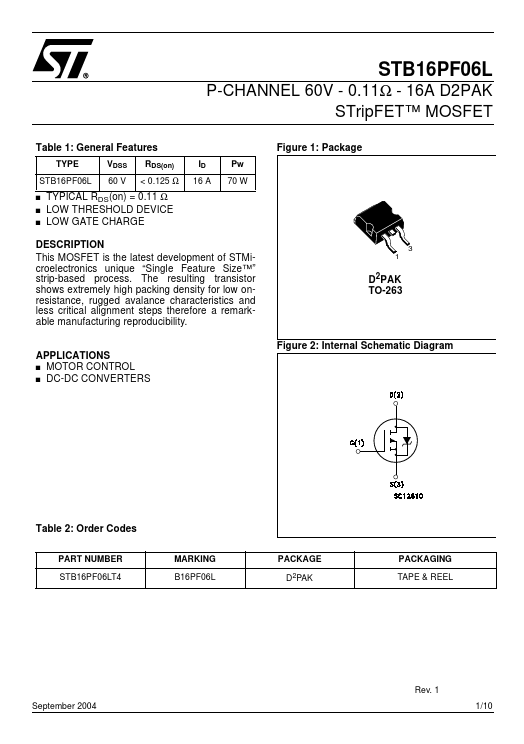
This MOSFET is the latest development of STMicroelectronics unique “Single Feature Size™” strip-based process. The resulting transistor shows extremely high packing density for low onresistance, rugged avalance characteristics and less critical alignment steps therefore a remarkable manufacturing reproducibility. D2PAK TO-263 Figure 2: Internal Schematic Diagram APPLICATIONS s MOTOR CONTROL s DC-DC CONVERTERS Table 2: Order Codes PART NUMBER STB16PF06LT4 MARKING B16PF06L PACKAGE D2PAK PACKAGING TAPE & REEL Rev. 1 September 2004 1/10 Table 3: Absolute Maximum ratings Symbol VDS VDGR VGS ID ID IDM ( ) PTOT dv/dt (1) EAS (2) Tj Tstg Parameter Drain-source Voltage (VGS = 0) Drain-gate Voltage (RGS = 20 kΩ) Gate-source Voltage Drain Current (continuous) at TC = 25°C Drain Current (continuous) at TC = 100°C Drain Current (pulsed) Total Dissipation at TC = 25°C Derating Factor Peak Diode Recovery voltage slope Single Pulse Avalanche Energy Operating Junction Temperature Storage Temperature Value 60 60 ± 16 16 11.4 64 70 0.4 20 250 - 55 to 175 Unit V V V A A A W W/°C V/ns m J °C ( ) Pulse width limited by safe operating area (1) ISD ≤ 16A, di/dt ≤100A/µs, VDD ≤ V(BR)DSS, Tj ≤ TJMAX. (2) Starting Tj = 25°C , ID = 8 A , VDD = 30 V Note:For the P-CHANNEL MOSFET actual polarity of voltages and current has to be reverse Table 4: Thermal Data Rthj-case Rthj-PCB(#) Tl Thermal Resistance Junction-case Max Thermal Resistance Junction-PCB Max Maximum Lead Temperature For Soldering Purpose (1.6 mm frrom case, for 10sec) 2.14 34 300 °C/W °C/W °C (#) When Mounted on 1 inch2 FR-4 board, 2 oz of Cu ELECTRICAL CHARACTERISTICS (TCASE =25°C UNLESS OTHERWISE SPECIFIED) Table 5: On/Off Symbol V(BR)DSS IDSS IGSS VGS(th) RDS(on) Parameter Drain-source Breakdown Voltage Zero Gate Voltage Drain Current (VGS =...