• Part: STB190NF04-1
  • Description: N-CHANNEL POWER MOSFET
  • Category: MOSFET
  • Manufacturer: STMicroelectronics
  • Size: 199.72 KB
Download STB190NF04-1 Datasheet PDF
STMicroelectronics
STB190NF04-1
STB190NF04-1 is N-CHANNEL POWER MOSFET manufactured by STMicroelectronics.
- Part of the STB190NF04 comparator family.
N This Power MOSFET is the latest development of STMicroelectronis unique "Single Feature Size™" strip-based process. The resulting transistor shows extremely high packing density for low onresistance, rugged avalanche characteristics and less critical alignment steps therefore a remarkable manufacturing reproducibility. 
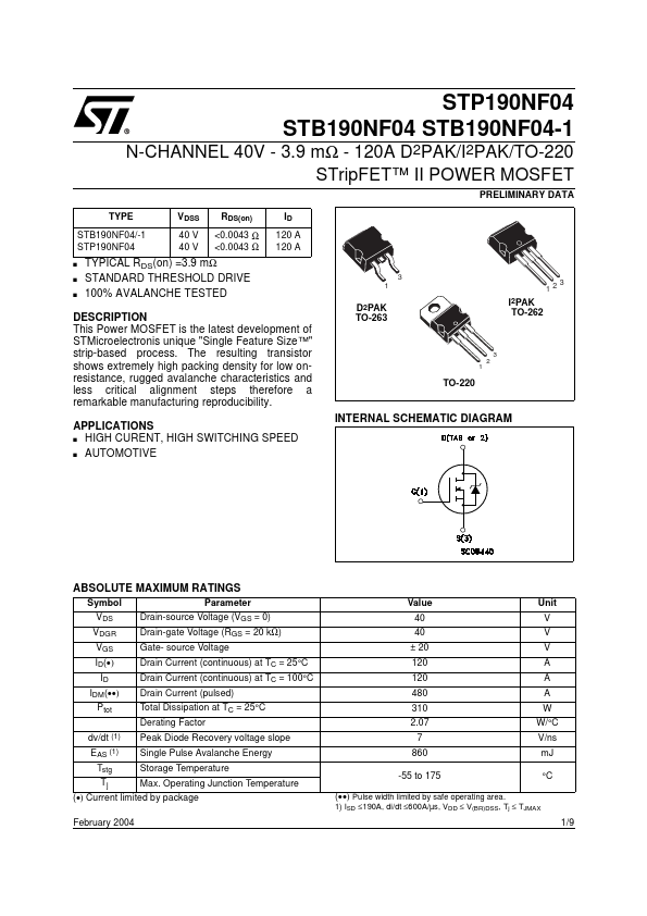
APPLICATIONS s HIGH CURENT, HIGH SWITCHING SPEED s AUTOMOTIVE D2PAK TO-263 I2PAK TO-262 3 1 2 TO-220 INTERNAL SCHEMATIC DIAGRAM ABSOLUTE MAXIMUM RATINGS Symbol VDS VDGR VGS ID(- ) ID IDM(- - ) Ptot dv/dt (1) Parameter Drain-source Voltage (VGS = 0) Drain-gate Voltage (RGS = 20 kΩ) Gate- source Voltage Drain Current (continuous) at TC = 25°C Drain Current (continuous) at TC = 100°C Drain Current (pulsed) Total Dissipation at TC = 25°C Derating Factor Peak Diode Recovery voltage slope Single Pulse Avalanche Energy Storage Temperature Max. Operating Junction Temperature Value 40 40 ± 20 120 120 480 310 2.07 7 860 -55 to 175 (- - ) Pulse width limited by safe operating area. Unit V V V A A A W W/°C V/ns m J °C EAS (1) Tstg Tj (- ) Current limited by package February 2004 1) ISD ≤190A, di/dt ≤600A/µs, VDD ≤ V(BR)DSS, Tj ≤ TJMAX 1/9 STB190NF04/-1 STP190NF04 THERMAL DATA Rthj-case Rthj-amb Tl Thermal Resistance Junction-case Thermal Resistance Junction-ambient Maximum Lead Temperature For Soldering Purpose Max Max Typ 0.48 50 300 °C/W °C/W °C ELECTRICAL CHARACTERISTICS (Tcase = 25 °C unless otherwise specified) OFF Symbol V(BR)DSS IDSS Parameter Drain-source Breakdown Voltage Zero Gate Voltage Drain Current (VGS = 0) Gate-body Leakage Current (VDS = 0) Test Conditions ID = 250 µA VGS = 0 Min. 40 1 10 ±100 Typ. Max. Unit V µA µA n A VDS = Max Rating VDS = Max Rating TC = 125°C VGS = ± 20V IGSS ON (- ) Symbol VGS(th) RDS(on) Parameter Gate Threshold Voltage Static Drain-source On Resistance Test Conditions VDS = VGS VGS = 10 V ID = 250 µA ID = 95A Min. 2 0.0039 Typ. Max. 4 0.0043 Unit V Ω DYNAMIC Symbol gfs (- ) Ciss Coss Crss Parameter Forward...