STB21NM50N-1 Overview
Key Specifications
Package: TO-262-3
Mount Type: Through Hole
Pins: 3
Max Operating Temp: 150 °C
Description
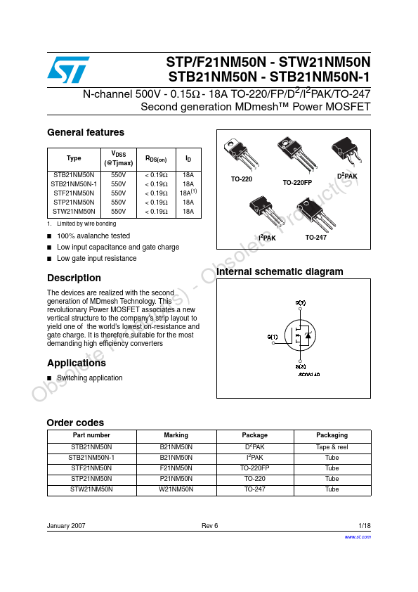
The STx21NM50N is realized with the second generation of MDmesh Technology. This revolutionary MOSFET associates a new vertical structure to the Company's strip layout to yield one of the world's lowest on-resistance and gate charge.
Key Features
- 100% AVALANCHE TESTED LOW INPUT CAPACITANCE AND GATE CHARGE LOW GATE INPUT RESISTANCE 3 12