• Part: STB45NF06L
  • Description: N-CHANNEL POWER MOSFET
  • Category: MOSFET
  • Manufacturer: STMicroelectronics
  • Size: 374.15 KB
Download STB45NF06L Datasheet PDF
STMicroelectronics
STB45NF06L
STB45NF06L is N-CHANNEL POWER MOSFET manufactured by STMicroelectronics.
N 
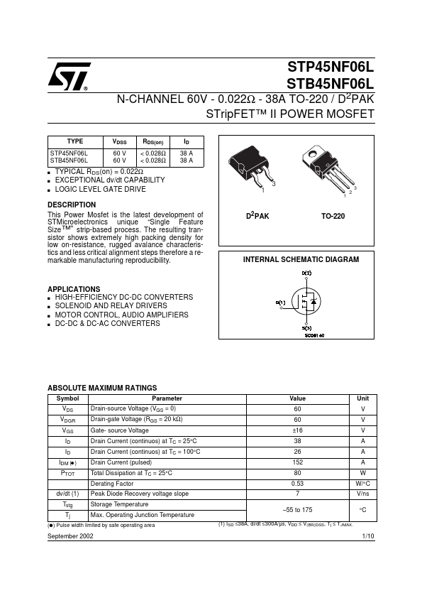
This Power Mosfet is the latest development of STMicroelectronics unique “Single Feature Size™” strip-based process. The resulting transistor shows extremely high packing density for low on-resistance, rugged avalance characteristics and less critical alignment steps therefore a remarkable manufacturing reproducibility. D2PAK TO-220 INTERNAL SCHEMATIC DIAGRAM APPLICATIONS s HIGH-EFFICIENCY DC-DC CONVERTERS s SOLENOID AND RELAY DRIVERS s MOTOR CONTROL, AUDIO AMPLIFIERS s DC-DC & DC-AC CONVERTERS ABSOLUTE MAXIMUM RATINGS Symbol VDS VDGR VGS ID ID IDM ( ) PTOT dv/dt (1) Tstg Tj Parameter Drain-source Voltage (VGS = 0) Drain-gate Voltage (RGS = 20 kΩ) Gate- source Voltage Drain Current (continuos) at TC = 25°C Drain Current (continuos) at TC = 100°C Drain Current (pulsed) Total Dissipation at TC = 25°C Derating Factor Peak Diode Recovery voltage slope Storage Temperature Max. Operating Junction Temperature Value 60 60 ±16 38 26 152 80 0.53 7 - 55 to 175 (1) ISD ≤38A, di/dt ≤ 300A/µs, VDD ≤ V(BR)DSS, Tj ≤ T JMAX. Unit V V V A A A W W/°C V/ns °C (q ) Pulse width limited by safe operating area September 2002 1/10 STP45NF06L - STB45NF06L THERMAL DATA Rthj-case Rthj-amb Tl Thermal Resistance Junction-case Max Thermal Resistance Junction-ambient Max Maximum Lead Temperature For Soldering Purpose 1.87 62.5 300 °C/W °C/W °C AVALANCHE CHARACTERISTICS Symbol IAR EAS Parameter Avalanche Current, Repetitive or Not-Repetitive (pulse width limited by Tj max) Single Pulse Avalanche Energy (starting Tj = 25 °C, ID = IAR, VDD = 50 V) Max Value 38 135 Unit A m J ELECTRICAL CHARACTERISTICS (TCASE = 25 °C UNLESS OTHERWISE SPECIFIED) OFF Symbol V(BR)DSS IDSS IGSS Parameter Drain-source Breakdown Voltage Zero Gate Voltage Drain Current (VGS = 0) Gate-body Leakage Current (VDS = 0) Test Conditions ID = 250 µA, VGS = 0 VDS = Max Rating VDS = Max Rating, TC = 125 °C VGS = ±16V Min. 60 1 10 ±100 Typ. Max. Unit V µA µA n A ON (1) Symbol VGS(th) RDS(on) Parameter Gate Threshold...