STB45NF3LL Overview
Key Specifications
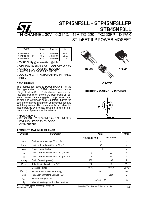
Package: D2PAK
Mount Type: Surface Mount
Pins: 3
Max Operating Temp: 175 °C
Description
This application specific Power MOSFET is the third genaration of STMicroelectronics unique “Single Feature Size™” strip-based process. The resulting transistor shows the best trade-off between on-resistance ang gate charge.
Key Features
- STB45NF3LL THERMAL DATA TO-220 D2PAK Rthj-case Rthj-amb Tl