STB5NC50-1
STB5NC50-1 is N-CHANNEL POWER MOSFET manufactured by STMicroelectronics.
- Part of the STB5NC50 comparator family.
- Part of the STB5NC50 comparator family.
e Power MESH™II is the evolution of the first generation of MESH OVERLAY™. The layout refinements introduced greatly improve the Ron- area figure of merit while keeping the device at the leading edge for what concerns swithing speed, gate charge and ruggedness.
I2PAK
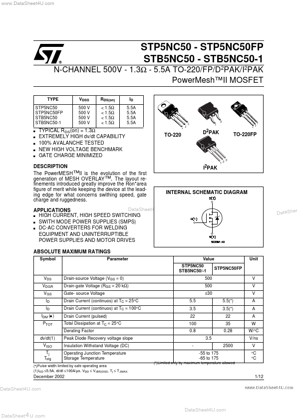
INTERNAL SCHEMATIC DIAGRAM
. APPLICATIONS s HIGH CURRENT, HIGH SPEED SWITCHING s SWITH MODE POWER SUPPLIES (SMPS) s DC-AC CONVERTERS FOR WELDING EQUIPMENT AND UNINTERRUPTIBLE POWER SUPPLIES AND MOTOR DRIVES
ABSOLUTE MAXIMUM RATINGS
Symbol Parameter Value STP5NC50 STB5NC50/-1 VDS VDGR VGS ID ID IDM ( ) PTOT dv/dt(1) VISO Tj Tstg Drain-source Voltage (VGS = 0) Drain-gate Voltage (RGS = 20 kΩ) Gate- source Voltage Drain Current (continuos) at TC = 25°C Drain Current (continuos) at TC = 100°C Drain Current (pulsed) Total Dissipation at TC = 25°C Derating Factor Peak Diode Recovery voltage slope Insulation Withstand Voltage (DC) Operating Junction Temperature Storage Temperature -55 to 175 -65 to 175
(- )Limited only by maximum temperature allowed
Data She e
Unit
STP5NC50FP V V V 5.5(- ) 3.5(- ) 22 35 0.28 A A A W W/°C V/ns 2500 V °C °C
500 500 ±30 5.5 3.5 22 100 0.8 3.5
(- )Pulse width limited by safe operating area (1)ISD ≤5.5A, di/dt ≤ 100A/µs, VDD ≤ V(BR)DSS, Tj ≤ T JMAX.
December 2002
1/12
.
. Data Sheet 4 U .
..
STP5NC50
- STP5NC50FP
- STB5NC50
- STB5NC50-1
THERMAL DATA
TO-220 D2PAK I2PAK Rthj-case Rthj-amb Tl Thermal Resistance Junction-case Max Thermal Resistance Junction-ambient Max Maximum Lead Temperature For Soldering Purpose 1.25 62.5 300 TO-220FP 3.57 °C/W °C/W °C
AVALANCHE CHARACTERISTICS
Symbol IAR EAS Parameter Avalanche Current, Repetitive or Not-Repetitive (pulse width limited by Tj max) Single Pulse Avalanche Energy (starting Tj = 25 °C, ID = IAR, VDD = 50 V) Max Value 5.5 280 Unit A m J
ELECTRICAL CHARACTERISTICS (TCASE = 25 °C UNLESS OTHERWISE SPECIFIED) OFF
Symbol V(BR)DSS IDSS IGSS Parameter Drain-source Breakdown Voltage Zero Gate Voltage Drain Current (VGS = 0) Gate-body...