STB60NH02L
STB60NH02L is N-CHANNEL Power MOSFET manufactured by STMicroelectronics.
NH02L utilizes the latest advanced design rules of ST’s proprietary STrip FET™ technology. This is suitable fot the most demanding DC-DC converter application where high efficiency is to be achieved.
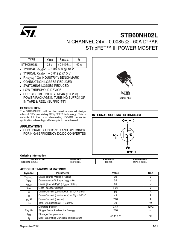
INTERNAL SCHEMATIC DIAGRAM
APPLICATIONS s SPECIFICALLY DESIGNED AND OPTIMISED FOR HIGH EFFICIENCY DC/DC CONVERTES
Ordering Information
SALES TYPE STB60NH02LT4 MARKING B60NH02L PACKAGE TO-263 PACKAGING TAPE & REEL
ABSOLUTE MAXIMUM RATINGS
Symbol Vspike(1) VDS VDGR VGS ID ID IDM(2) Ptot EAS (3) Tstg Tj Parameter Drain-source Voltage Rating Drain-source Voltage (VGS = 0) Drain-gate Voltage (RGS = 20 kΩ) Gate- source Voltage Drain Current (continuous) at TC = 25°C Drain Current (continuous) at TC = 100°C Drain Current (pulsed) Total Dissipation at TC = 25°C Derating Factor Single Pulse Avalanche Energy Storage Temperature Max. Operating Junction Temperature Value 30 24 24 ± 20 60 43 240 70 0.47 280 -55 to 175 Unit V V V V A A A W W/°C m J °C
September 2003
1/11
THERMAL DATA
Rthj-case Rthj-amb Tl Thermal Resistance Junction-case Thermal Resistance Junction-ambient Maximum Lead Temperature For Soldering Purpose Max Max 2.14 62.5 300 °C/W °C/W °C
ELECTRICAL CHARACTERISTICS (TCASE = 25 °C UNLESS OTHERWISE SPECIFIED) OFF
Symbol V(BR)DSS IDSS IGSS Parameter Drain-source Breakdown Voltage Zero Gate Voltage Drain Current (VGS = 0) Gate-body Leakage Current (VDS = 0) Test Conditions ID = 25 m A, VGS = 0 VDS = 20 V VDS = 20 V VGS = ± 20V Min. 24 1 10 ±100 Typ. Max. Unit V µA µA n A
TC = 125°C
ON (4)
Symbol VGS(th) RDS(on) Parameter Gate Threshold Voltage Static Drain-source On Resistance Test Conditions VDS = VGS VGS = 10 V VGS = 5 V ID = 250 µA ID = 30 A ID = 15 A Min. 1 Typ. 1.8 0.0085 0.012 Max. 2.5 0.0105 0.020 Unit V Ω Ω
DYNAMIC
Symbol gfs (4) Ciss Coss Crss RG Parameter Forward Transconductance Input Capacitance Output Capacitance Reverse Transfer Capacitance Gate Input Resistance Test Conditions VDS = 15 V ID = 25 A Min. Typ. 27 1400 400 55 Max. Unit S p F p F...