Datasheet Summary
N-CHANNEL 700V
- 7.3Ω
- 1.4A TO-220/FP/DPAK/IPAK Zener-Protected PowerMESH™III MOSFET
TYPE STP2NC70Z STP2NC70ZFP STD1NC70Z STD1NC70Z-1 s s s s s
STP2NC70Z, STP2NC70ZFP STD1NC70Z, STD1NC70Z-1
VDSS 700 700 700 700 V V V V
RDS(on) < 8.5 < 8.5 < 8.5 < 8.5 Ω Ω Ω Ω
ID 1.4 A 1.4 A 1.4 A 1.4 A
Pw 50 W 25 W 45 W 45 W
3 2
TYPICAL RDS(on) = 7.3 Ω EXTREMELY HIGH dv/dt CAPABILITY 100% AVALANCHE TESTED GATE CHARGE MINIMIZED VERY LOW INTRINSIC CAPACITANCES
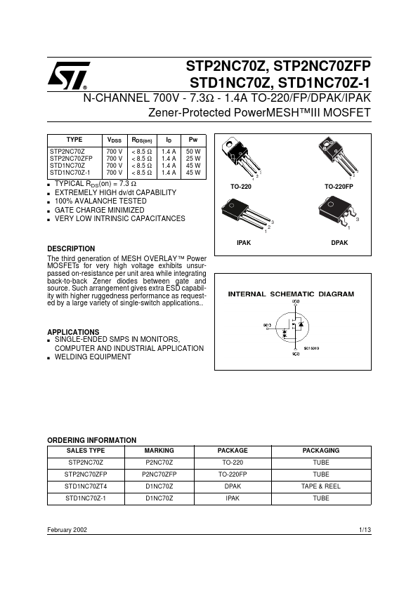
TO-220
TO-220FP
3 2 1
3 1
IPAK
DPAK
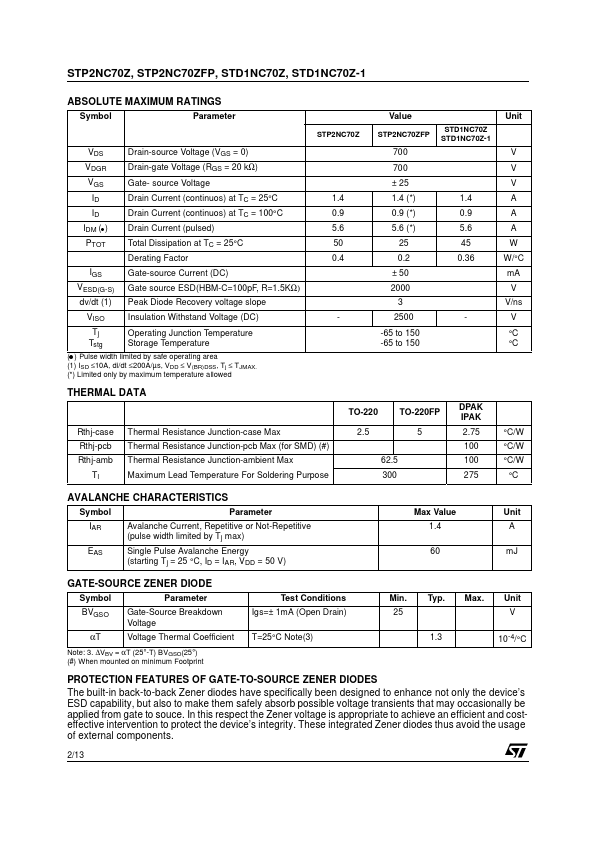
DESCRIPTION The third generation of MESH OVERLAY ™ Power MOSFETs for very high voltage exhibits unsurpassed on-resistance per unit area while integrating back-to-back Zener diodes between gate and...