STD2NM60
STD2NM60 is N-CHANNEL MOSFET manufactured by STMicroelectronics.
N-CHANNEL 600V
- 2.8Ω
- 2A DPAK/IPAK Zener-Protected MDmesh™Power MOSFET
TYPE STD2NM60 STD2NM60-1 s s s s
STD2NM60 STD2NM60-1
VDSS 600V 600V
RDS(on) < 3.2 Ω < 3.2 Ω
ID 2A 2A s s
TYPICAL RDS(on) = 2.8 Ω HIGH dv/dt AND AVALANCHE CAPABILITIES 100% AVALANCHE TESTED LOW INPUT CAPACITANCE AND GATE CHARGE LOW GATE INPUT RESISTANCE TIGHT PROCESS CONTROL AND HIGH MANUFACTORING YIELDS
3 1
2 1
DPAK TO-252
IPAK TO-251
DESCRIPTION The MDmesh™ is a new revolutionary MOSFET technology that associates the Multiple Drain process with the pany’s Power MESH™ horizontal layout. The resulting product has an outstanding low on-resistance, impressively high dv/dt and excellent avalanche characteristics. The adoption of the pany’s proprietary strip technique yields overall dynamic performance that is significantly better than that of similar pletition’s products. APPLICATIONS The MDmesh™ family is very suitable for increase the power density of high voltage converters allowing system miniaturization and higher efficiencies. ABSOLUTE MAXIMUM RATINGS
Symbol VDS VDGR VGS ID ID IDM (q) PTOT VESD(G-S) dv/dt(1) Tstg Tj Parameter Drain-source Voltage (VGS = 0) Drain-gate Voltage (RGS = 20 kΩ) Gate- source Voltage Drain Current (continuous) at TC = 25°C Drain Current (continuous) at TC = 100°C Drain Current (pulsed) Total Dissipation at TC = 25°C Derating Factor Gate source ESD(HBM-C=100p F, R=1.5KΩ) Peak Diode Recovery voltage slope Storage Temperature Max. Operating Junction Temperature
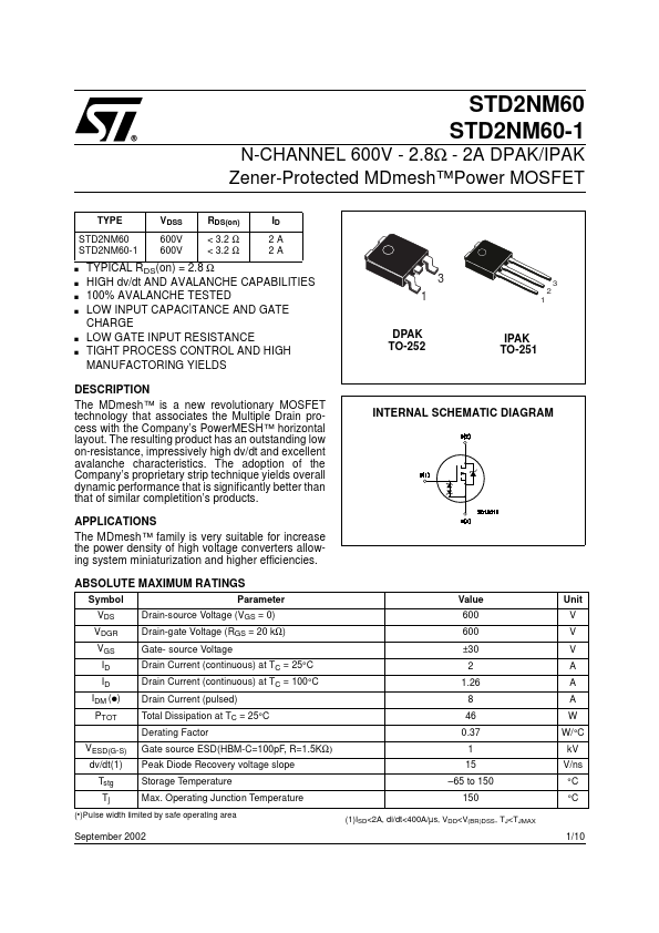
INTERNAL SCHEMATIC DIAGRAM
Value 600 600 ±30 2 1.26 8 46 0.37 1 15
- 65 to 150 150
(1)ISD<2A, di/dt<400A/µs, VDD<V(BR)DSS , TJ<TJMAX
Unit V V V A A A W W/°C k V V/ns °C °C
(- )Pulse width limited by safe operating area
September 2002
1/10
STD2NM60/STD2NM60-1
THERMAL DATA
Rthj-case Rthj-amb Tl Thermal Resistance Junction-case Max Thermal Resistance Junction-ambient Max Maximum Lead Temperature For Soldering Purpose 2.73 62.5 300 °C/W °C/W °C
AVALANCHE CHARACTERISTICS
Symbol IAR EAS...