Datasheet4U Logo Datasheet4U.com

STGB10NB40LZ Datasheet N-channel IGBT

Manufacturer: STMicroelectronics

Overview: STGB10NB40LZ N-CHANNEL CLAMPED 20A - D²PAK INTERNALLY CLAMPED PowerMESH™ IGBT TYPE STGB10NB40LZ s s s s s s VCES CLAMPED VCE(sat) < 1.

General Description

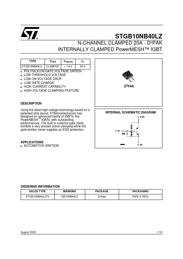
Using the latest high voltage technology based on a patented strip layout, STMicroelectronics has designed an advanced family of IGBTs, the PowerMESH™ IGBTs, with outstanding performances.

The built in collector-gate zener exhibits a very precise active clamping while the gate-emitter zener supplies an ESD protection.

INTERNAL SCHEMATIC DIAGRAM APPLICATIONS s AUTOMOTIVE IGNITION ORDERING INFORMATION SALES TYPE STGB10NB40LZT4 MARKING GB10NB40LZ PACKAGE D2PAK PACKAGING TAPE & REEL August 2003 1/10 STGB10NB40LZ ABSOLUTE MAXIMUM RATINGS Symbol VCES VECR VGE IC IC ICM ( ) Eas PTOT ESD Tstg Tj Parameter Collector-Emitter Voltage (VGS = 0) Emitter-Collector Voltage Gate-Emitter Voltage Collector Current (continuos) at TC = 25°C Collector Current (continuos) at TC = 100°C Collector Current (pulsed) Single Pulse Energy Tc = 25°C Total Dissipation at TC = 25°C Derating Factor ESD (Human Body Model) Storage Temperature Operating Junction Temperature Value CLAMPED 18 CLAMPED 20 10 40 300 150 1 4 – 55 to 175 Unit V V V A A A mJ W W/°C KV °C ( )Pulse width limited by safe operating area THERMAL DATA Rthj-case Rthj-amb Thermal Resistance Junction-case Max Thermal Resistance Junction-ambient Max 1 62.5 °C/W °C/W ELECTRICAL CHARACTERISTICS (TCASE = 25 °C UNLESS OTHERWISE SPECIFIED) OFF Symbol BV(CES) BV(ECR) BVGE ICES IGES RGE Parameter Clamped Voltage Emitter Collector Break-down Voltage Gate Emitter Break-down Voltage Collector cut-off Current (VGE = 0) Gate-Emitter Leakage Current (VCE = 0) Gate Emitter Resistance Test Conditions IC = 2 mA, VGE = 0, Tj= - 40°C to 150°C IC = 75 mA, Tj= 25°C IG = ± 2 mA VCE = 15 V, VGE= 0 ,Tj= 150 °C VCE= 200 V, VGE= 0 ,Tj= 15

STGB10NB40LZ Distributor