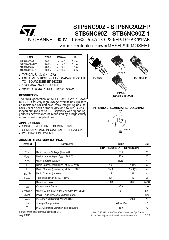
STP6NC90Z
STP6NC90Z is N-CHANNEL Power MOSFET manufactured by STMicroelectronics.
N-CHANNEL 900V
- 1.55Ω
- 5.4A TO-220/FP/D²PAK/I²PAK Zener-Protected Power MESH™III MOSFET
TYPE STP6NC90Z STP6NC90ZFP STB6NC90Z STB6NC90Z-1 s s
- STP6NC90ZFP STB6NC90Z
- STB6NC90Z-1
VDSS 900 V 900 V 900 V 900 V
RDS(on) < 1.9 < 1.9 < 1.9 < 1.9 Ω Ω Ω Ω
ID 5.4 5.4 5.4 5.4 A A A A
3 1 s s
TYPICAL RDS(on) = 1.55Ω EXTREMELY HIGH dv/dt AND CAPABILITY GATE TO
- SOURCE ZENER DIODES 100% AVALANCHE TESTED VERY LOW GATE INPUT RESISTANCE
D²PAK
3 2
TO-220
TO-220FP
DESCRIPTION The third generation of MESH OVERLAY™ Power MOSFETs for very high voltage exhibits unsurpassed on-resistance per unit area while integrating back-toback Zener diodes between gate and source. Such arrangement gives extra ESD capability with higher ruggedness performance as requested by a large variety of single-switch applications. APPLICATIONS s SINGLE-ENDED SMPS IN MONITORS, PUTER AND INDUSTRIAL APPLICATION s WELDING EQUIPMENT...