STATS ChipPAC FBGA-SD
This capability uses existing assembly infrastructure, which results in more functional integration with lower overall package cost. The use of the latest packaging materials allows this package to meet JEDEC Moisture Resistance Test Level 2a with Lead-free reflow conditions.| Part No. | FBGA-SD |
|---|---|
| Datasheet | FBGA-SD Download |
| Manufacturer | STATS ChipPAC |
| Description | Fine Pitch Ball Grid Array |
| Buy | Stock & Price |
FEATURES
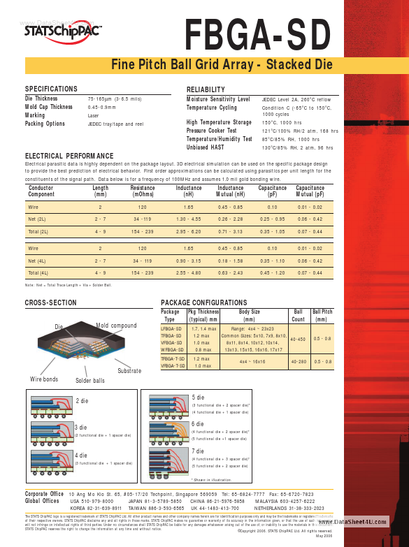
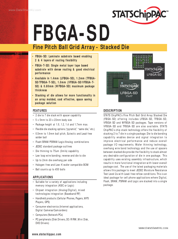
● 2 die to 7 die stack with spacer capability● 5 x 5mm to 23 x 23mm body size
● Package height at 1.0, 1.2, 1.4 and 1.7mm max.
● Flexible die stacking options (“pyramid,” “same die,” etc.)
● 0.5mm to 1.0mm ball pitch, Eutectic and Lead-free solder ball
● Flash/SRAM/PSRAM/Logic/Analog combinations
● JEDEC standard package outlines
● Die thinning to 75um (3mils) capability
● Low loop wire bonding; reverse and die to die
● Up to 2mm die overhang per side
● Halogen-free and Low-K wafer compatible BOM
● Ball counts up to 450 balls
DESCRIPTION
STATS ChipPAC’s Fine Pitch Ball Grid Array Stacked Die (FBGA-SD) offering includes LFBGA-SD, TFBGA-SD, VFBGA-SD and WFBGA-SD packages. Tape versions of VFBGA-SD and TFBGA-SD are also available. STATS ChipPAC’s chip stack technology offers the flexibility of stacking 2 to 7 die in a single package. Die to die bonding capability enables device and signal integration to improve electrical performance and reduce overall package I/O requirements.