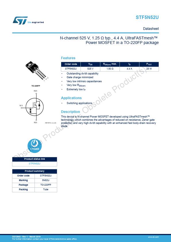
5N52U Overview
Key Features
- Outstanding dv/dt capability
- Gate charge minimized
- Very low intrinsic capacitances
- Very low RDS(on)
- Extremely low trr 1.50 Ω 4.4 A 25 W te P Applications le
- Switching applications o G(1) bs Description
- Pulse width limited by safe operating area. b
- ISD ≤ 4.4 A, di/dt ≤ 400 A/µs, VDS peak < V(BR)DSS, VDD = 80% V(BR)DSS t(s)
- O Symbol uc Rthj-case rod Rthj-amb Table
- Thermal data Parameter 2.8 17.6 25 20 2.5 -55 to 150 2.8 Value 5 62.5 olete P Symbol Obs IAR Table