STMicroelectronics 74LX1G07
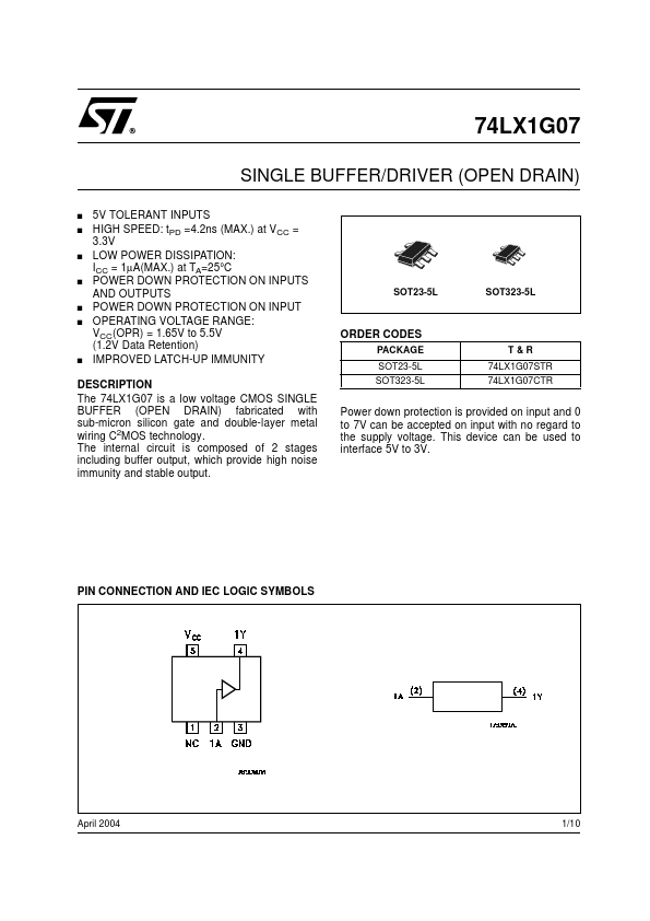
The 74LX1G07 is a low voltage CMOS SINGLE BUFFER (OPEN DRAIN) fabricated with sub-micron silicon gate and double-layer metal wiring C2MOS technology. The internal circuit is composed of 2 stages including buffer output, which provide high noise immunity and stable output. This device can be used to interface 5V to 3V.| Part No. | 74LX1G07 |
|---|---|
| Datasheet | 74LX1G07 Download |
| Manufacturer |  STMicroelectronics |
| Description | SINGLE BUFFER/DRIVER |
| Buy | Stock & Price |
DESCRIPTION
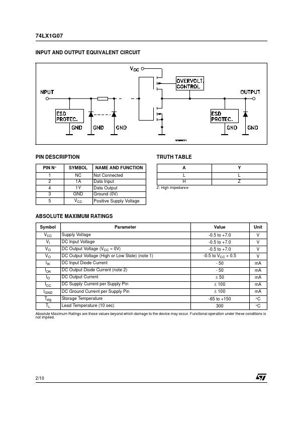
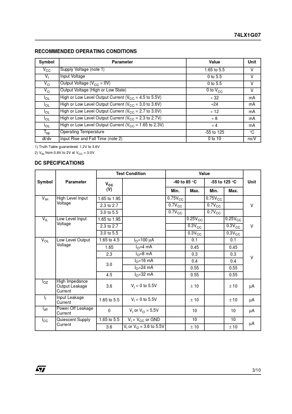
Power down protection is provided on input and 0 to 7V can be accepted on input with no regard to the supply voltage. This device can be used to interface 5V to 3V. PIN CONNECTION AND IEC LOGIC SYMBOLS April 2004 1/10 74LX1G07 INPUT AND OUTPUT EQUIVALENT CIRCUIT PINDESCRIPTION
PIN N° 1 2 4 3 5 SYMBOL NC 1A 1Y GND VCC NAME AND FUNCTION Not Connected Data Input Data Output Ground (0V) Positive Supply Voltage TRUTH TABLE A L H Z: High Impedance Y L ZABSOLUTE MAXIMUM RATINGS
Symbol VCC VI VO VO IIK IOK IO ICC IGND Tstg TL Supply Voltage DC Input Voltage DC Output Voltage (VCC = 0V) DC Output Voltage (High or Low State) (note 1) DC Input Diode Current DC Output Diode Current (note 2) DC Output Current DC Supply Current per Supply Pin DC Ground Current per Supply Pin Storage Temperature Lead Temperature (10 sec) Parameter Value -0.5 to +7.0 -0.5 to +7.0 -0.5 to +7.0 -0.5 to VCC + 0.5 - 50 - 50 ± 50 ± 100 ± 100 -65 to +150 300 Unit V V V V mA mA mA mA mA °C °CABSOLUTE MAXIMUM RATINGS
are those values beyond which damage to the device may occur.