GWT30V60DF
GWT30V60DF is IGBT manufactured by STMicroelectronics.
STGB30V60DF, STGP30V60DF, STGW30V60DF, STGWT30V60DF
Trench gate field-stop IGBT, V series 600 V, 30 A very high speed
- production data
3 1
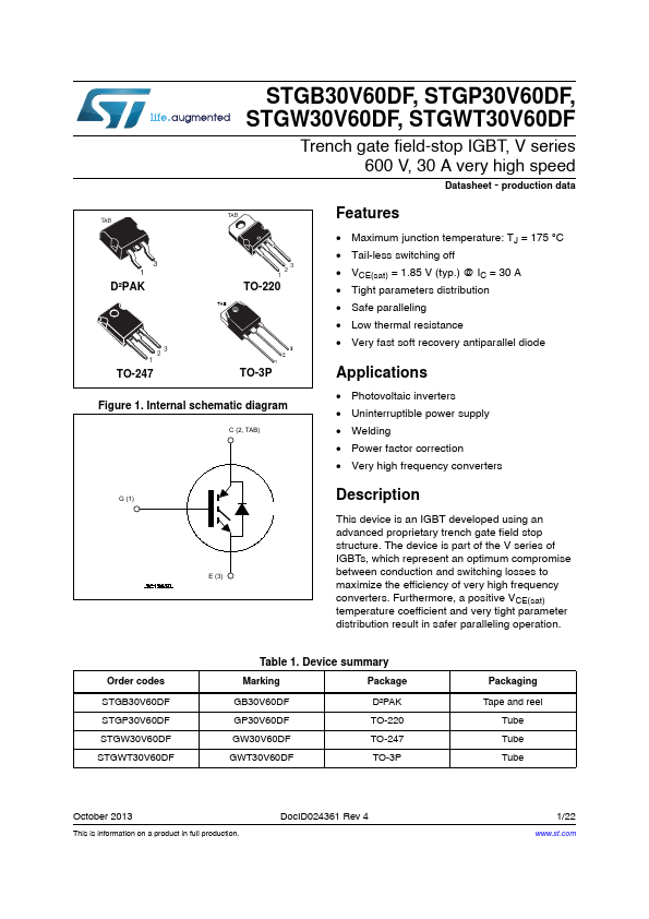
D²PAK
3 2 1
TO-220
3 2 1
TO-247
3 2 1
TO-3P
Figure 1. Internal schematic diagram
C (2, TAB)
Features
- Maximum junction temperature: TJ = 175 °C
- Tail-less switching off
- VCE(sat) = 1.85 V (typ.) @ IC = 30 A
- Tight parameters distribution
- Safe paralleling
- Low thermal resistance
- Very fast soft recovery antiparallel diode
Applications
- Photovoltaic inverters
- Uninterruptible power supply
- Welding
- Power factor correction
- Very high frequency converters
G (1) Description
This device is an IGBT developed using an advanced proprietary trench gate field stop structure. The device is part of the V series of IGBTs, which represent an optimum promise E (3) between conduction and switching losses to maximize the efficiency of very high frequency converters. Furthermore, a positive...