STMicroelectronics HCF4503
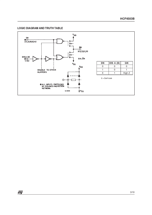
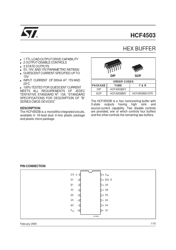
The HCF4503B is a monolithic integrated circuits, available in 16-lead dual in-line plastic package and plastic micro package. The HCF4503B is a hex noninverting buffer with 3-state outputs having high sink and source-current capability. This is a stress rating only and functional operation ofthe device atthese or any other conditions above those indicated in the operational sections of this specification is not implied.| Part No. | HCF4503 |
|---|---|
| Datasheet | HCF4503 Download |
| Manufacturer |  STMicroelectronics |
| Description | HEX BUFFER |
| Buy | Stock & Price |
DESCRIPTION
OF ”B” SERIES CMOS DEVICES” s s DIP ORDER CODES PACKAGE DIP SOP TUBE HCF4503BEY HCF4503BM1 SOP T& R HCF4503M013TRDESCRIPTION
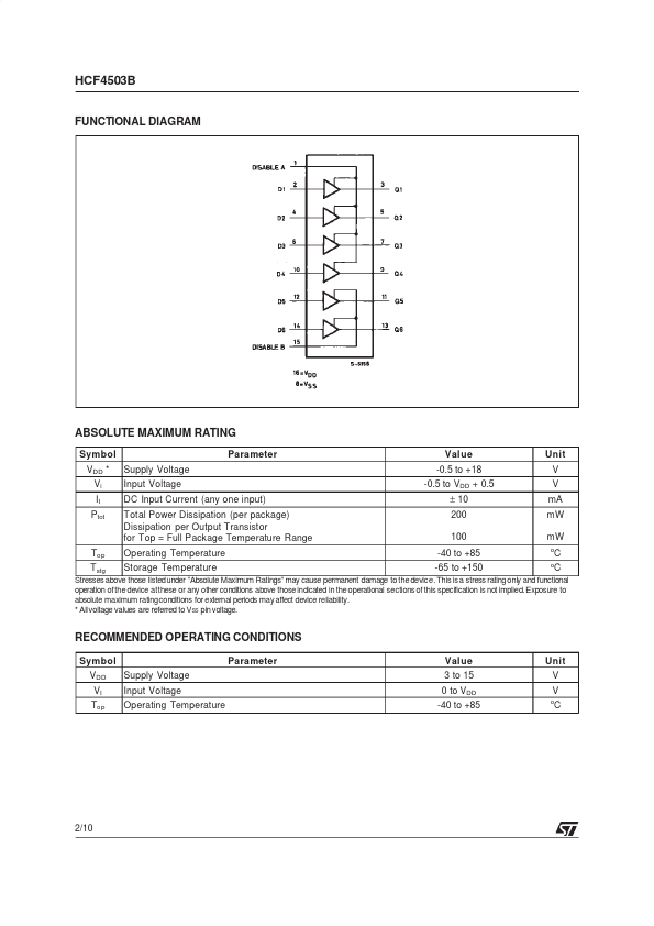
Two disable controls are provided, one of which controls four buffers and the other controls the remaining two buffers. PIN CONNECTION February 2000 1/10 HCF4503B FUNCTIONAL DIAGRAM ABSOLUTE MAXIMUM RATING Symbol VDD * Vi II Ptot Supply Voltage Input Voltage DC Input Current (any one input) Total Power Dissipation (per package) Dissipation per Output Transistor for Top = Full Package Temperature Range Operating Temperature Storage Temperature Parameter Value -0.5 to +18 -0.5 to VDD + 0.5 ± 10 200 100 -40 to +85 -65 to +150 Unit V V mA mW mW o o Top Tstg C C Stresses above those listedunder ”ABSOLUTE MAXIMUM RATINGS
” may cause permanent damage to the device. Exposure to absolute maximum ratingconditions for external periods may affect device reliability. * Allvoltage values are referred to VSS pin voltage. RECOMMENDED OPERATING CONDITIONS Symbol VDD V...