STMicroelectronics IRFBC40
This power MOSFET is designed using the company’s consolidated strip layout-based MESH OVERLAY™ process. This technology matches and improves the performances compared with standard parts from various sources.| Part No. | IRFBC40 |
|---|---|
| Datasheet | IRFBC40 Download |
| Manufacturer |  STMicroelectronics |
| Description | N-Channel Power MOSFET |
| Buy | Stock & Price |
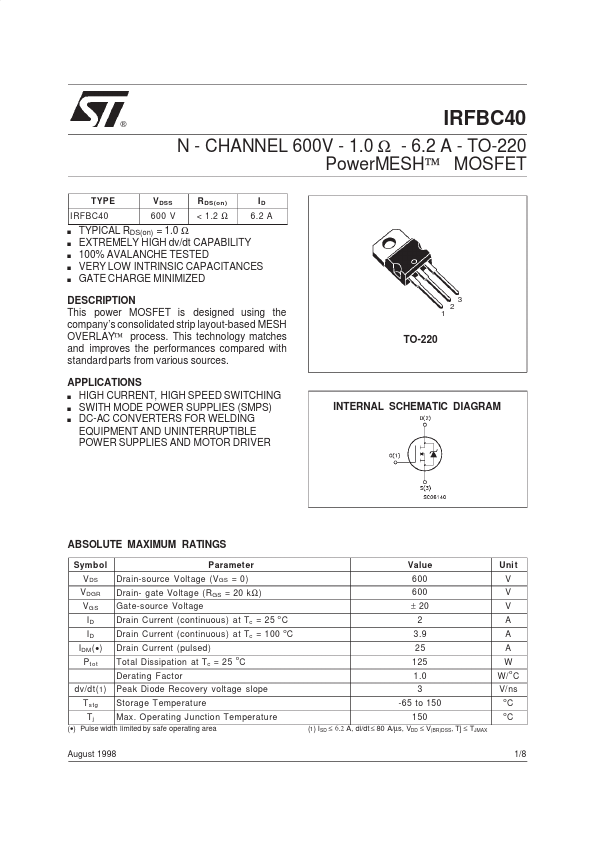
DESCRIPTION
APPLICATIONS
s HIGH CURRENT, HIGH SPEED SWITCHING s SWITH MODE POWER SUPPLIES (SMPS) s DC-AC CONVERTERS FOR WELDING EQUIPMENT AND UNINTERRUPTIBLE POWER SUPPLIES AND MOTOR DRIVER 1 TO-220 INTERNAL SCHEMATIC DIAGRAMABSOLUTE MAXIMUM RATINGS
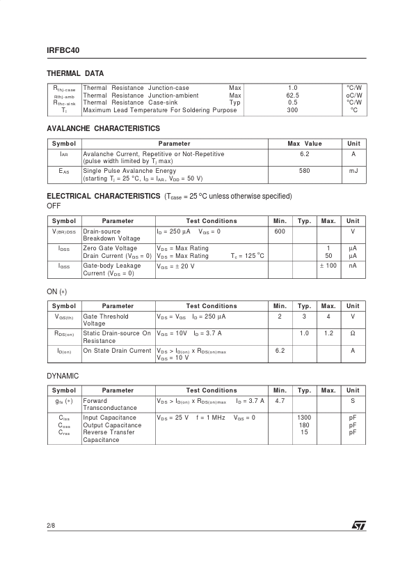
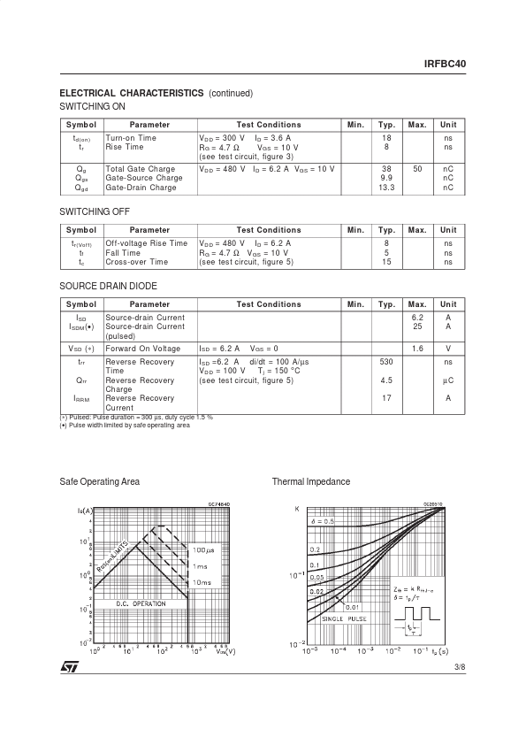
Symbol V DS V DGR V GS ID ID IDM (● ) P t ot dv/dt( 1 ) T stg Tj Parameter Drain-source Voltage (V GS = 0) Drain- gate Voltage (R GS = 20 k Ω ) Gate-source Voltage Drain Current (continuous) at Tc = 25 C Drain Current (continuous) at Tc = 100 C Drain Current (pulsed) Total Dissipation at Tc = 25 C Derating F actor Peak Diode Recovery voltage slope Storage T emperature Max. O perating Junction Temperature o o o Value 600 600 ± 20 2 3.9 25 125 1.0 3 -65 to 150 150 (1) ISD ≤ 6.2 A, di/dt ≤ 80 A/µs, VDD ≤ V(BR)DSS, Tj ≤ TJMAX Uni t V V V A A A W W/ C V/ ns o o o C C (●) Pulse width limited by safe operating area August 1998 1/8 IRFBC40 THERMAL DATA R t hj-ca se Rthj -amb R thc- si nk Tl Thermal Resistance Junction-case Max Thermal Resistance...