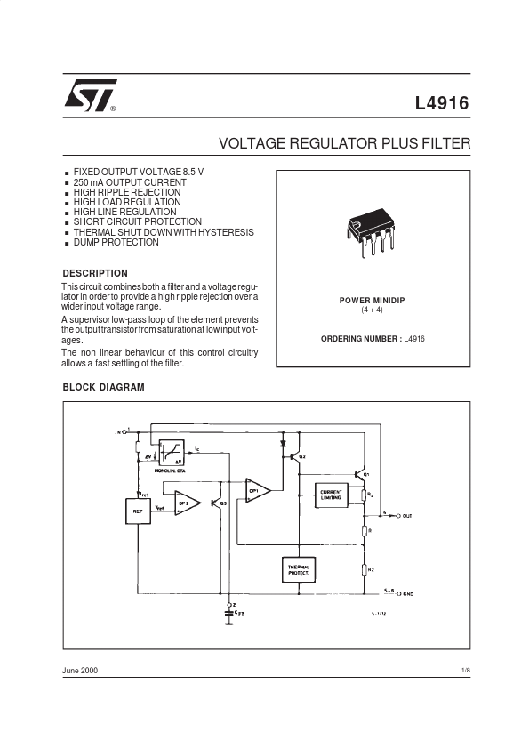
DESCRIPTION
This circuit combinesboth a filter and a voltageregulator in order to provide a high ripple rejection over a wider input voltage range. A supervisor low-pass loop of the element prevents the outputtransistor from saturationat low input voltages. The non linear behaviour of this control circuitry allows a fast settling of the filter. BLOCK DIAGRAM POW ER MINIDIP (4 + 4) ORDERING NUMBER : L4916 June 2000 1/8 L4916 PIN CONNECTION (top view) ABSOLUTE MAXIMUM RATINGS
Symbol Vi Vi IO Ptot Tstg, Tj Peak Input Voltage (300 ms) DC Input Voltage Output Current Power Dissipation Storage and Junction Temperature Parameter Value 40 28 Internally Limited Internally Limited – 40 to 150 °C Unit V V THERMAL DATA Symbol Parameter R th j-amb Thermal Resistance Junction-ambient Rth j-pins Thermal Resistance Junction-pins Max Max Value 80 20 Unit °C/W °C/W 2/8 L4916 ELECTRICAL CHARACTERISTICS
(Tamb =25 °C; Vi = 13.5 V, testcircuit of fig. 1, unlessotherwise specified) Symbol Vi VO ∆V I/O ∆ VO ∆ VO Parameter Input Voltage Output Voltage Controlled Voltage Vi = 12 to 18 V IO = 5 to 150 mA 8.1 8.5 1.6 1 50 Test Conditions Min. STMicroelectronics