DESCRIPTION
A supervisor low-pass loop of the element prevents the output transistor from saturation at low input vol tages. BLOCK DIAGRAM PENTAWATT ORDERING NUMBER : L4918 October 1988 1/6 L4918 PIN CONNECTION (top view) Figure 1 : Application and Test Circuit. ABSOLUTE MAXIMUM RATINGS
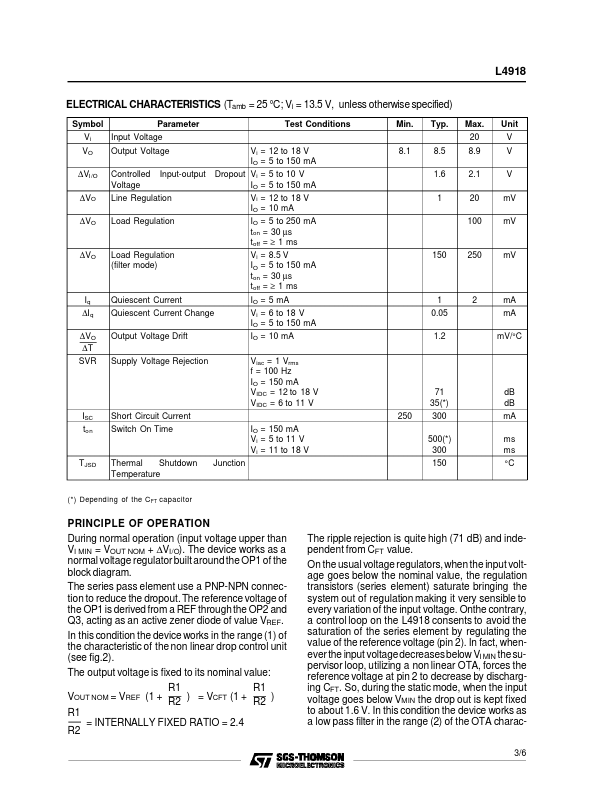
Symbol Vi Vi IO Ptot Tstg, Tj Peak Input Voltage (300 ms) DC Input Voltage Output Current Power Dissipation Storage and Junction Temperature Parameter Value 40 28 Internally Limited Internally Limited – 40 to 150 °C Unit V V THERMAL DATA Symbol Parameter Max Value 4 Unit °C/W Rth j-case Thermal Resistance Junction-case 2/6 L4918 ELECTRICAL CHARACTERISTICS
(Tamb = 25 °C; Vi = 13.5 V, unless otherwise specified) Symbol Vi VO ∆VI/O ∆ VO ∆ VO Parameter Input Voltage Output Voltage Controlled Voltage Input-output Vi = 12 to 18 V IO = 5 to 150 mA Dropout Vi = 5 to 10 V IO = 5 to 150 mA Vi = 12 to 18 V IO = 10 mA IO = 5 to 250 mA ton = 30 µs toff = ≥ 1 ms Vi = 8.5 V IO = 5 to 150 mA ton = 30 µs toff = ≥ 1 ms I... STMicroelectronics