DESCRIPTION
FEATURES
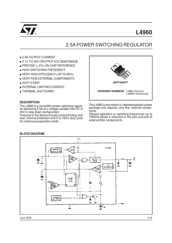
of the device include current limiting, soft start, thermal protection and 0 to 100% duty cycle for continuous operation mode. Efficient operation at switching frequencies up to 150KHz allows a reduction in the size and cost of external filter components. BLOCK DIAGRAM June 2000 1/16 L4960 PIN CONNECTION (Top view) ABSOLUTE MAXIMUM RATINGS
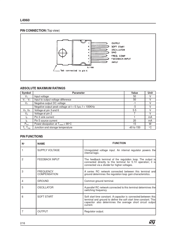
Symbol V1 V1 - V7 V7 V3, V6 V2 I3 I5 Ptot Tj, Tstg Parameter Input voltage Input to output voltage difference Negative output DC voltage Negative output peak voltage at t = 0.1µs; f = 100KHz Voltage at pin 3 and 6 Voltage at pin 2 Pin 3 sink current Pin 5 source current Power dissipation at Tcase ≤ 90°C Junction and storage temperature Value 50 50 -1 -5 5.5 7 1 20 15 -40 to 150 Unit V V V V V V mA mA W °C PIN FUNCTIONS N° 1 NAME SUPPLY VOLTAGE FUNCTION Unregulated voltage input. An internal regulator powers the internal logic. The feedback terminal of the regulation loop. The output is connected directly to this terminal for 5.1V operation; it is connected via a divider for higher voltages. STMicroelectronics