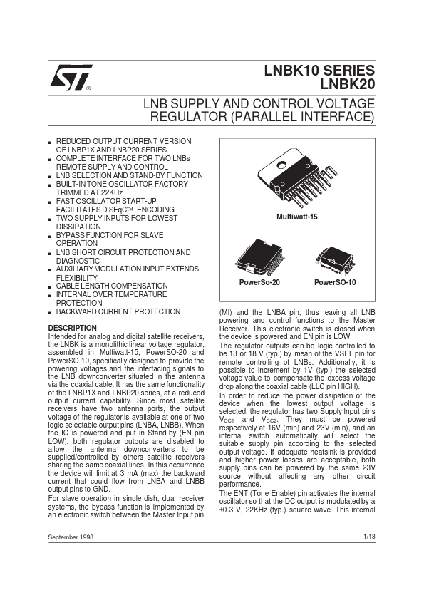
DESCRIPTION
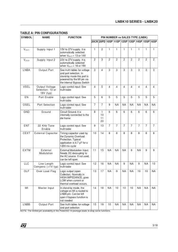
Intended for analog and digital satellite receivers, Since most satellite receivers have two antenna ports, the output voltage of the regulator is available at one of two logic-selectable output pins (LNBA, LNBB). In this occurrence the device will limit at 3 mA (max) the backward current that could flow from LNBA and LNBB output pins to GND. For slave operation in single dish, dual receiver systems, the bypass function is implemented by an electronic switch between the Master Input pin September 1998 (MI) and the LNBA pin, thus leaving all LNB powering and control functions to the Master Receiver. This electronic switch is closed when the device is powered and EN pin is LOW. The regulator outputs can be logic controlled to be 13 or 18 V (typ.) by mean of the VSEL pin for remote controlling of LNBs. Additionally, it is possible to increment by 1V (typ.) the selected voltage value to compensate the excess voltage drop along the coaxial cable (LLC pin HIGH). In order to reduce the power dissipation of the device when the lowest output voltage is selected, the regulator has two Supply Input pins VCC1 and VCC2. STMicroelectronics