FEATURES
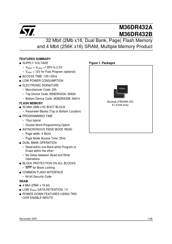
SUMMARY s SUPPLY VOLTAGE – VDDF = VDDS =1.65V to 2.2V s s s Figure 1. Packages – VPPF = 12V for Fast Program (optional) ACCESS TIME: 100,120ns LOW POWER CONSUMPTION ELECTRONIC SIGNATURE – Manufacturer Code: 20h – Top Device Code, M36DR432A: 00A0h – Bottom Device Code, M36DR432B: 00A1h FBGA FLASH MEMORY s 32 Mbit (2Mb x16) BOOT BLOCK – Parameter Blocks (Top or Bottom Location) s Stacked LFBGA66 (ZA) 8 x 8 ball array PROGRAMMING TIME – 10µs typical – Double Word Programming Option s ASYNCRONOUS PAGE MODE READ – Page width: 4 Word – Page Mode Access Time: 35ns s DUAL BANK OPERATION – Read within one Bank while Program or Erase within the other – No Delay between Read and Write Operations s BLOCK PROTECTION ON ALL BLOCKS – WPF for Block Locking COMMON FLASH INTERFACE – 64 bit Security Code s s s s SRAM 4 Mbit (256K x 16 bit) LOW VDDS DATA RETENTION: 1V POWER DOWN FEATURES
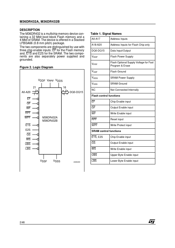
USING TWO CHIP ENABLE INPUTS November 2001 1/46 M36DR432A, M36DR432B DESCRIPTION
The two components are also separately power supplied and grounded. STMicroelectronics