M36L0T7050B0 Overview
Key Specifications
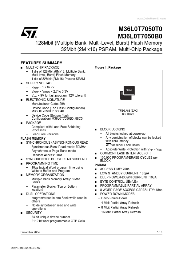
Package: TFBGA
Max Voltage (typical range): 1.95 V
Min Voltage (typical range): 1.7 V
Length: 10 mm
Key Features
- SUPPLY VOLTAGE – VDDF = 1.7 to 2V – VDDP = VDDQ = 2.7 to 3.3V – VPP = 9V for fast program (12V tolerant)
- PACKAGE – Compliant with Lead-Free Soldering Processes – Lead-Free Versions FLASH MEMORY
- SYNCHRONOUS / ASYNCHRONOUS READ – Synchronous Burst Read mode: 50MHz – Asynchronous Page Read mode – Random Access: 90ns
- SYNCHRONOUS BURST READ SUSPEND
- PROGRAMMING TIME – 10µs typical Word program time using Write to Buffer and Program
- MEMORY ORGANIZATION – Multiple Bank Memory Array: 8 Mbit Banks – Parameter Blocks (Top or Bottom location)
- DUAL OPERATIONS – program/erase in one Bank while read in others – No delay between read and write operations
- SECURITY – 64 bit unique device number – 2112 bit user programmable OTP Cells
- COMMON FLASH INTERFACE (CFI)
- 100,000 PROGRAM/ERASE CYCLES per BLOCK PSRAM