M36W0R6030B0 Overview
Key Features
- Flash Memory – 1 die of 8 Mbit SRAM
- SUPPLY VOLTAGE – VDDF = VDDQ = VDDS = 1.7 to 1.95V
- LOW POWER CONSUMPTION
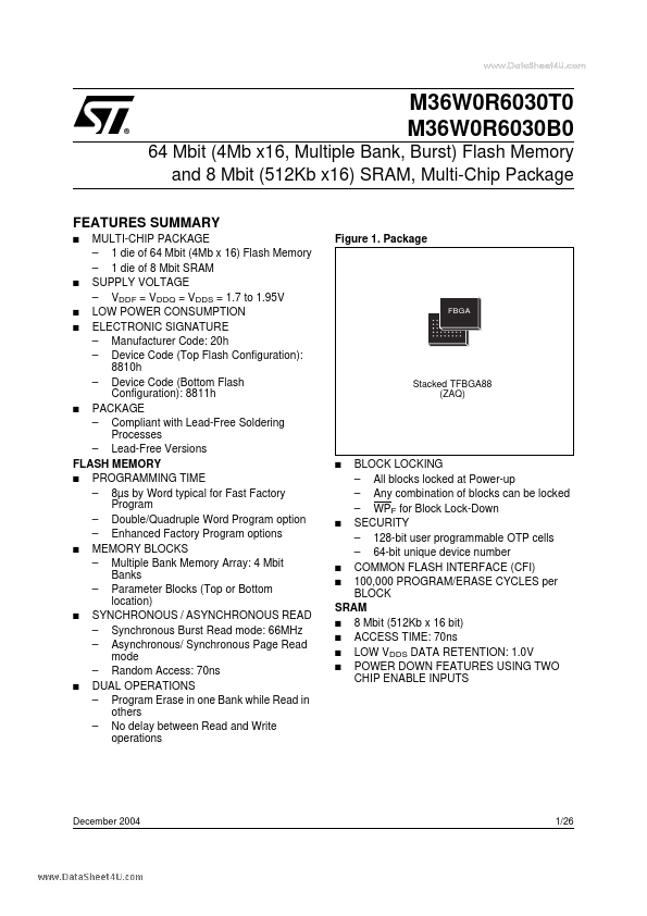
- PACKAGE – Compliant with Lead-Free Soldering Processes – Lead-Free Versions FLASH MEMORY
- PROGRAMMING TIME – 8µs by Word typical for Fast Factory Program – Double/Quadruple Word Program option – Enhanced Factory Program options
- MEMORY BLOCKS – Multiple Bank Memory Array: 4 Mbit Banks – Parameter Blocks (Top or Bottom location)
- SYNCHRONOUS / ASYNCHRONOUS READ – Synchronous Burst Read mode: 66MHz – Asynchronous/ Synchronous Page Read mode – Random Access: 70ns
- DUAL OPERATIONS – Program Erase in one Bank while Read in others – No delay between Read and Write operations
- SECURITY – 128-bit user programmable OTP cells – 64-bit unique device number
- COMMON FLASH INTERFACE (CFI)