DESCRIPTION
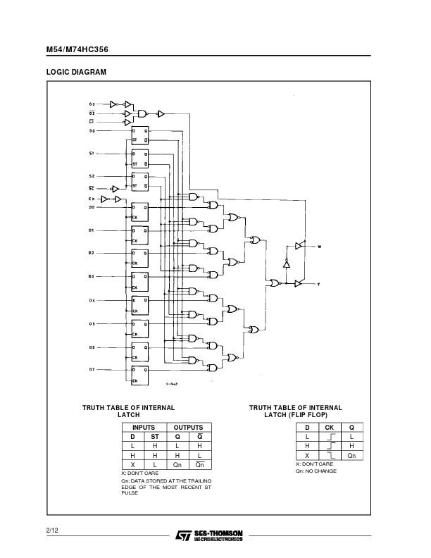
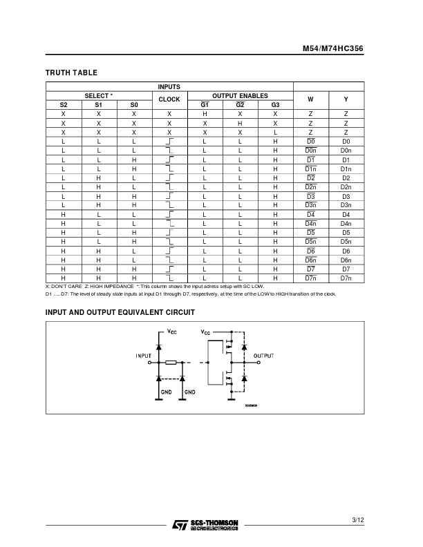
The one of eight input data will be provided on the Y output pin (noninverted output) and W output pin (inverted output) is determineted by the address data. The information at the data inputs (D0 to D7) is stored in the 8-bit flip-flop at the positive going edge of clock input (CLOCK). The information at the address inputs (S0 to S2) is stored in the 3-bit latch at the negative pulse on SC input. These outputs are disabled to be high-impedance when input G1 is held high, input G2 is held high or input G3 is held low. This device is suitable for interfacing with bus lines in a bus organized system. The M54/74HC356 is similar in function to the M54/74HC354, which has an 8-bit latch as the data register instead of an 8-bit flip-flop. All inputs are equipped with protection circuits against static discharge and transient excess voltage. January 1993 NC = No Internal Connection 1/12 M54/M74HC356 LOGIC DIAGRAM TRUTH TABLE OF INTERNAL LATCH INPUTS D ST L H X H H L OUTPUTS Q Q L H... STMicroelectronics