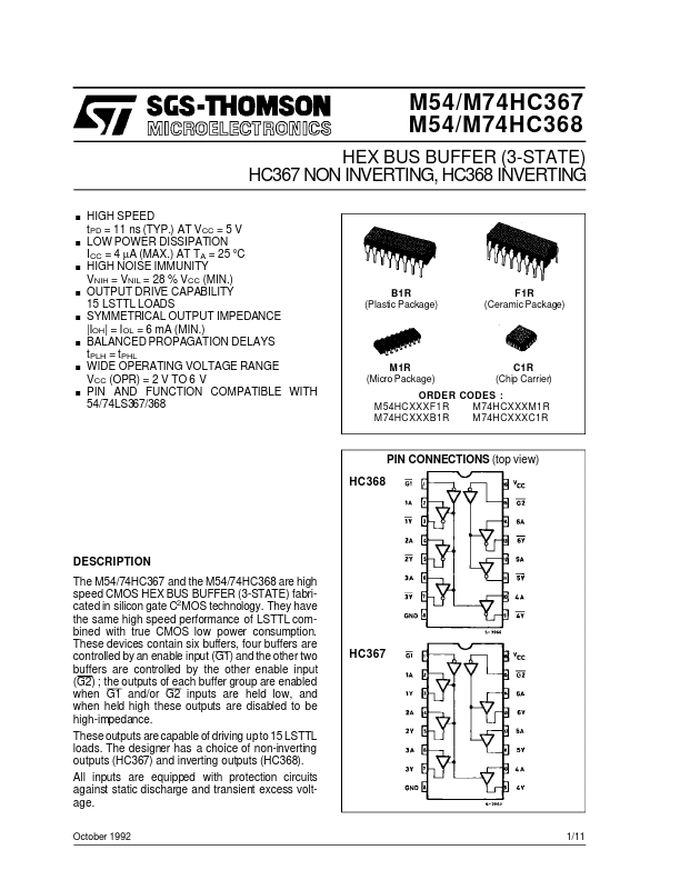
DESCRIPTION
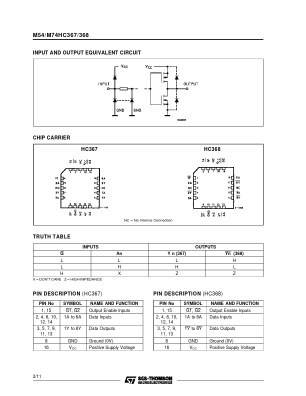
These outputs are capable of driving up to 15 LSTTL loads. The designer has a choice of non-inverting outputs (HC367) and inverting outputs (HC368). All inputs are equipped with protection circuits against static discharge and transient excess voltage. October 1992 1/11 HC367 M54/M74HC367/368 INPUT AND OUTPUT EQUIVALENT CIRCUIT CHIP CARRIER HC367 HC368 NC = No Internal Connection TRUTH TABLE INPUTS G L L H X = DON’T CARE Z = HIGH IMPEDANCE OUTPUTS An L H X Y n (367) L H Z Yn (368) H L Z PIN DESCRIPTION
(HC367) PIN No 1, 15 2, 4, 6, 10, 12, 14 3, 5, 7, 9, 11, 13 8 16 SYMBOL G1, G2 1A to 6A 1Y to 6Y GND V CC NAME AND FUNCTION Output Enable Inputs Data Inputs Data Outputs Ground (0V) Positive Supply Voltage PIN DESCRIPTION
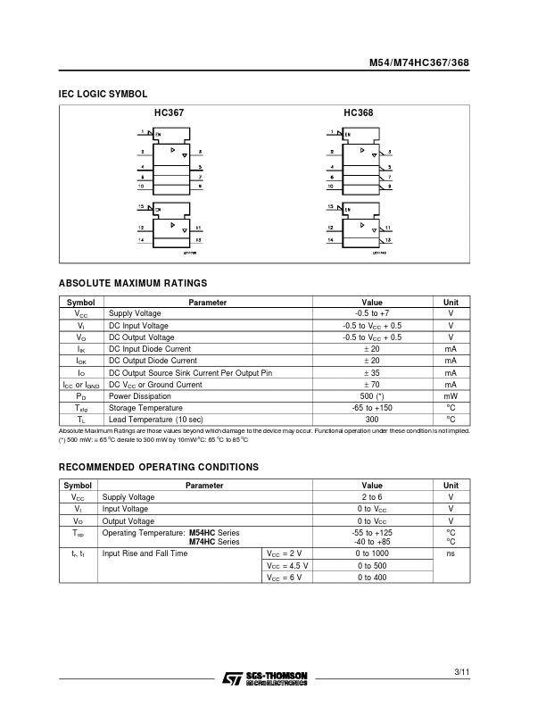
(HC368) PIN No 1, 15 2, 4, 6, 10, 12, 14 3, 5, 7, 9, 11, 13 8 16 SYMBOL G1, G2 1A to 6A 1Y to 6Y GND VCC NAME AND FUNCTION Output Enable Inputs Data Inputs Data Outputs Ground (0V) Positive Supply Voltage 2/11 M54/M74HC367/368 IEC LOGIC SYMBOL HC367 HC368 AB... STMicroelectronics