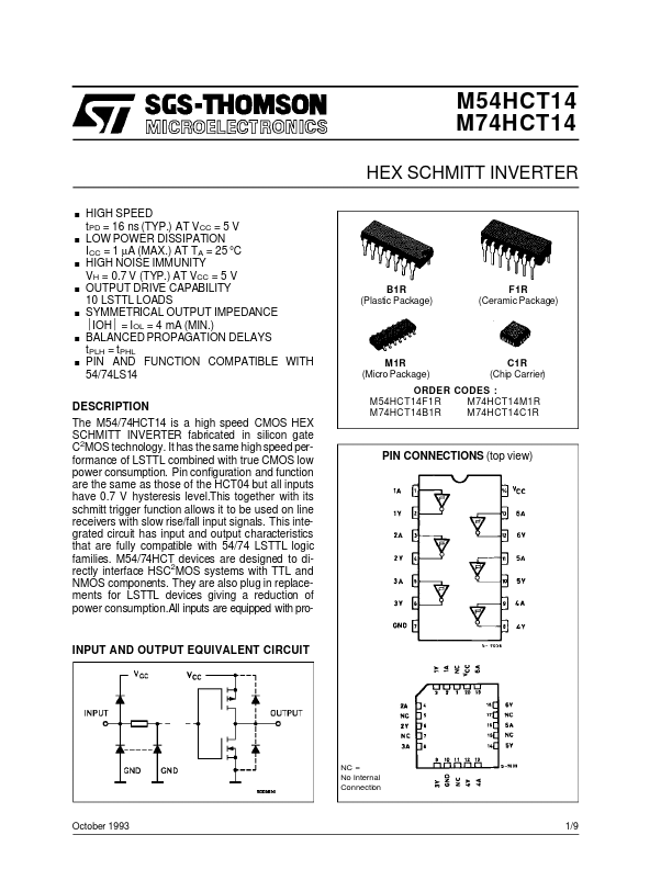
DESCRIPTION
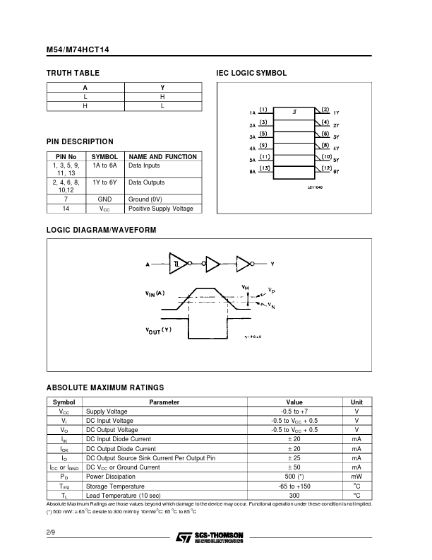
Pin configuration and function are the same as those of the HCT04 but all inputs have 0.7 V hysteresis level.This together with its schmitt trigger function allows it to be used on line receivers with slow rise/fall input signals. M54/74HCT devices are designed to directly interface HSC2MOS systems with TTL and NMOS components. They are also plug in replacements for LSTTL devices giving a reduction of power consumption.All inputs are equipped with pro- ORDER CODES : M54HCT14F1R M74HCT14M1R M74HCT14B1R M74HCT14C1R PIN CONNECTIONS (top view) INPUT AND OUTPUT EQUIVALENT CIRCUIT NC = No Internal Connection October 1993 1/9 M54/M74HCT14 TRUTH TABLE A L H Y H L IEC LOGIC SYMBOL PIN DESCRIPTION
PIN No 1, 3, 5, 9, 11, 13 2, 4, 6, 8, 10,12 7 14 SYMBOL 1A to 6A 1Y to 6Y GND VCC NAME AND FUNCTION Data Inputs Data Outputs Ground (0V) Positive Supply Voltage LOGIC DIAGRAM/WAVEFORM ABSOLUTE MAXIMUM RATINGS
Symbol VCC VI VO IIK IOK ICC IO or IGND PD Tstg TL Supply Voltage DC Input Voltage... STMicroelectronics