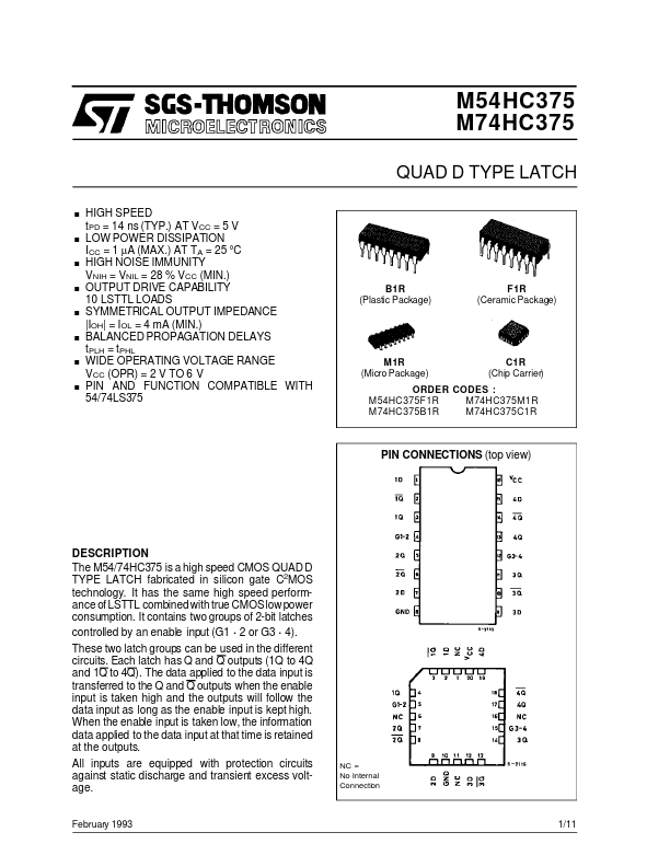
DESCRIPTION
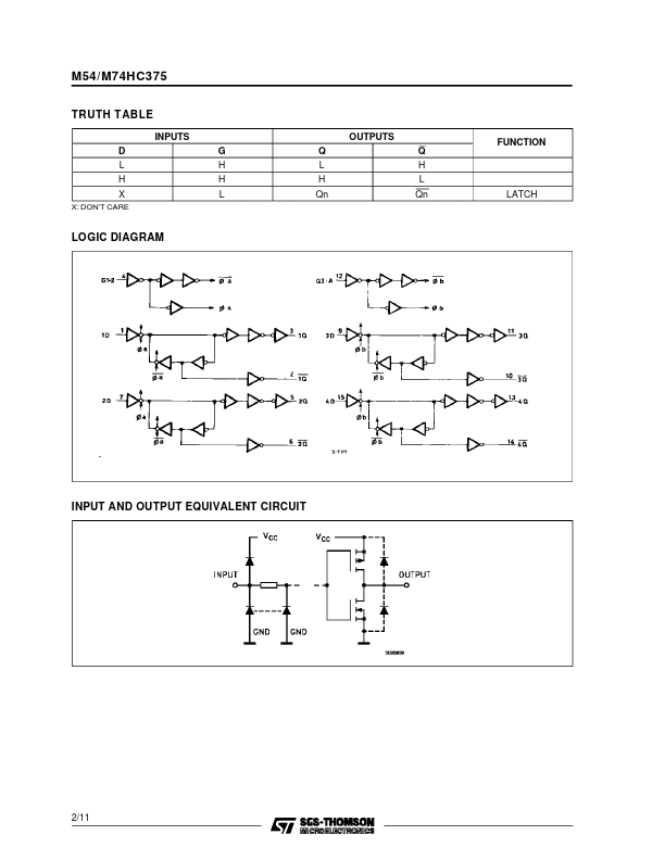
It contains two groups of 2-bit latches controlled by an enable input (G1 . 2 or G3 . 4). These two latch groups can be used in the different circuits. Each latch has Q and Q outputs (1Q to 4Q and 1Q to 4Q). The data applied to the data input is transferred to the Q and Q outputs when the enable input is taken high and the outputs will follow the data input as long as the enable input is kept high. When the enable input is taken low, the information data applied to the data input at that time is retained at the outputs. All inputs are equipped with protection circuits against static discharge and transient excess voltage. February 1993 NC = No Internal Connection 1/11 M54/M74HC375 TRUTH TABLE INPUTS D L H X X: DON’T CARE OUTPUTS G H H L Q L H Qn Q H L Qn FUNCTION LATCH LOGIC DIAGRAM INPUT AND OUTPUT EQUIVALENT CIRCUIT 2/11 M54/M74HC375 PIN DESCRIPTION
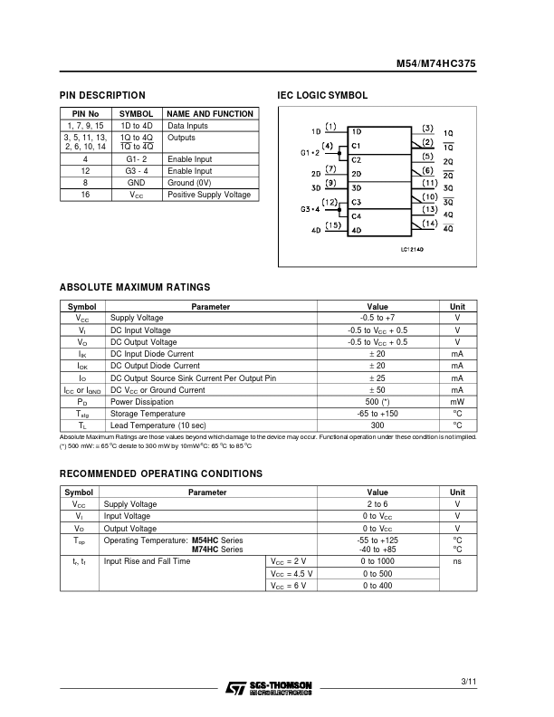
PIN No 1, 7, 9, 15 3, 5, 11, 13, 2, 6, 10, 14 4 12 8 16 SYMBOL 1D to 4D 1Q to 4Q 1Q to 4Q G1- 2 G3 - 4 GND V CC NAME AND FUN... STMicroelectronics