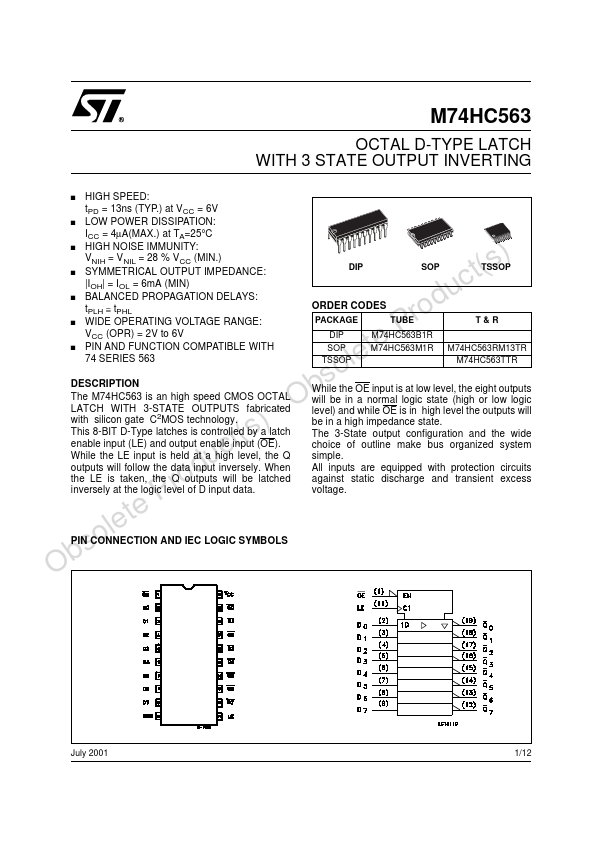
DESCRIPTION
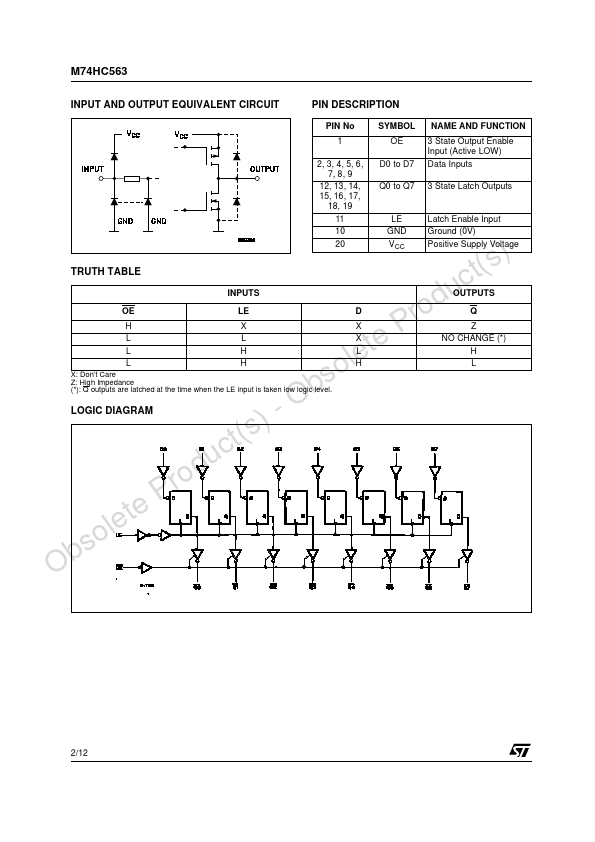
PIN No SYMBOL NAME AND FUNCTION 1 OE 3 State Output Enable Input (Active LOW) 2, 3, 4, 5, 6, D0 to D7 Data Inputs 7, 8, 9 12, 13, 14, 15, 16, 17, 18, 19 Q0 to Q7 3 State Latch Outputs 11 LE Latch Enable Input 10 GND Ground (0V) 20 t(s)TRUTH TABLE ucINPUTS dOE LE roH X PL L teL H leL H oX: Don’t Care sZ: High Impedance b(*): Q outputs are latched at the time when the LE input is taken low logic level. Obsolete Product(s) - OLOGIC DIAGRAM D X X L H VCC Positive Supply Voltage OUTPUTS Q Z NO CHANGE (*) H L 2/12 M74HC563 ABSOLUTE MAXIMUM RATINGS
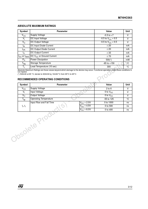
Symbol Parameter Value Unit VCC Supply Voltage -0.5 to +7 V VI DC Input Voltage -0.5 to VCC + 0.5 V VO DC Output Voltage -0.5 to VCC + 0.5 V IIK DC Input Diode Current ± 20 mA IOK DC Output Diode Current ± 20 mA IO DC Output Current ± 35 mA ICC or IGND DC VCC or Ground Current ± 70 mA PD Power Dissipation 500(*) mW )Tstg Storage Temperature -65 to +150 °C t(sTL Lead Temperature (10 sec) 300 °C ABSOLUTE MAXIMUM RATINGS
are those values beyond which damage to the device may occur. STMicroelectronics