FEATURES
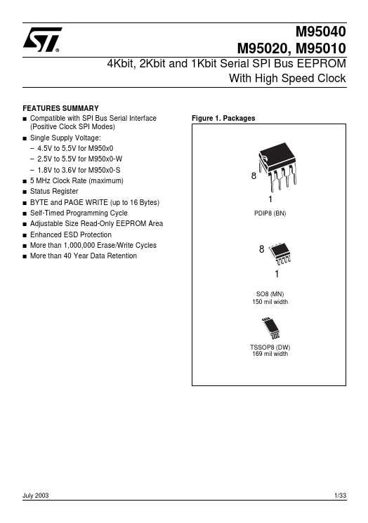
SUMMARY s Compatible with SPI Bus Serial Interface (Positive Clock SPI Modes) s Figure 1. Packages Single Supply Voltage: – 4.5V to 5.5V for M950x0 – 2.5V to 5.5V for M950x0-W – 1.8V to 3.6V for M950x0-S s s s s s s s s 5 MHz Clock Rate (maximum) Status Register BYTE and PAGE WRITE (up to 16 Bytes) Self-Timed Programming Cycle Adjustable Size Read-Only EEPROM Area Enhanced ESD Protection More than 1,000,000 Erase/Write Cycles More than 40 Year Data Retention 8 1 PDIP8 (BN) 8 1 SO8 (MN) 150 mil width TSSOP8 (DW) 169 mil width July 2003 1/33 M95040, M95020, M95010 SUMMARY DESCRIPTION
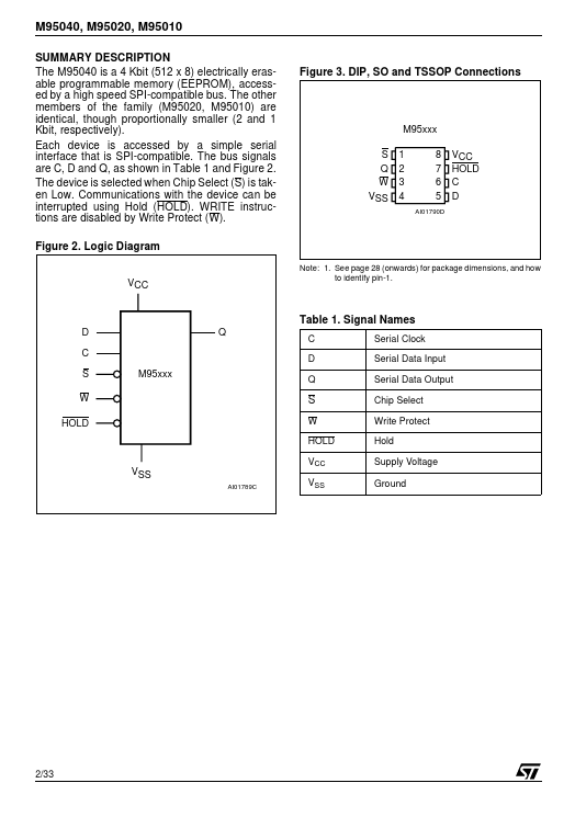
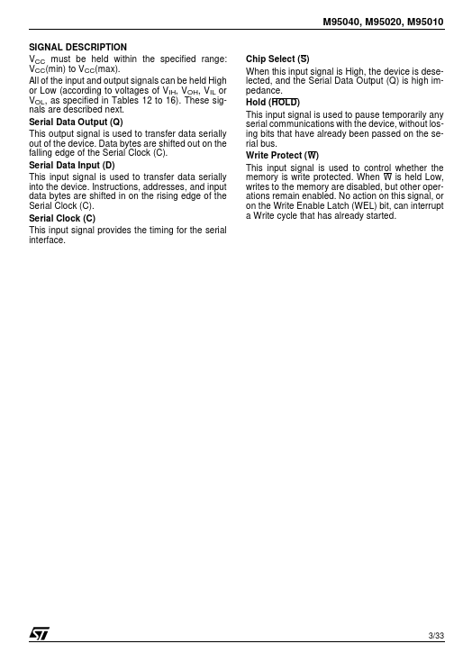
The bus signals are C, D and Q, as shown in Table 1 and Figure 2. The device is selected when Chip Select (S) is taken Low. Communications with the device can be interrupted using Hold (HOLD). WRITE instructions are disabled by Write Protect (W). Figure 2. Logic Diagram Note: 1. See page 28 (onwards) for package dimensions, and how to identify pin-1. Figure 3. DIP, SO and TSSOP Connections M95xxx S Q W VSS 1 2 3 4 8 7 6 5 AI01790D VCC HOLD C D VCC Table 1. STMicroelectronics