P11NM50N Overview
Key Specifications
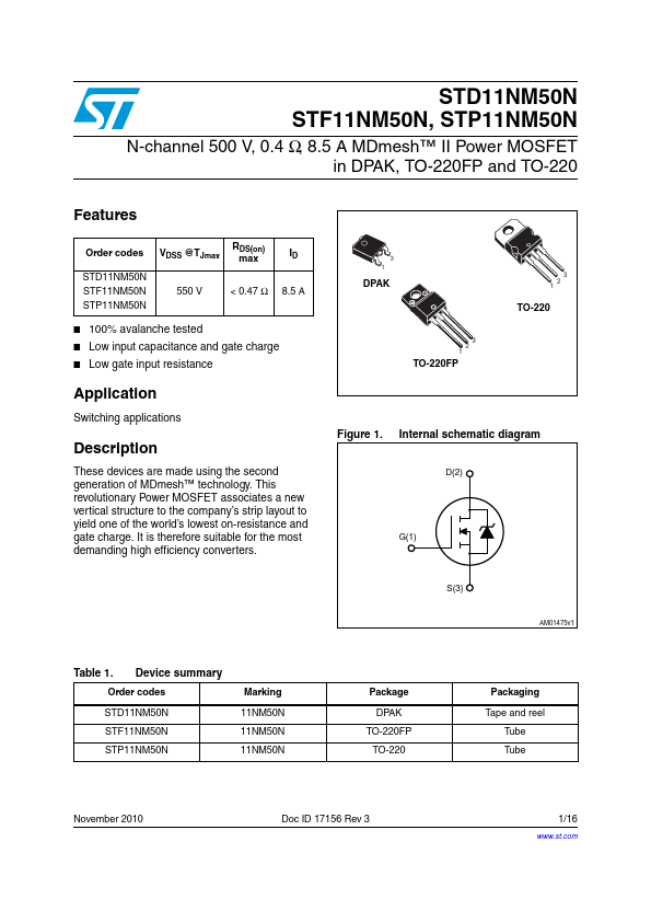
Package: TO-220
Mount Type: Through Hole
Pins: 3
Height: 15.75 mm
Description
These devices are made using the second generation of MDmesh™ technology. This revolutionary Power MOSFET associates a new vertical structure to the company’s strip layout to yield one of the world’s lowest on-resistance and gate charge.
Key Features
- 100% avalanche tested
- Low input capacitance and gate charge
- Low gate input resistance