STMicroelectronics STA5630
The STA5630 embeds high performance LNA minimizing external component count. The chip uses state of the art CMOS 65 nm technology. The magnitude bits are internally integrated in order to control the variable gain amplifiers.| Part No. | STA5630 |
|---|---|
| Datasheet | STA5630 Download |
| Manufacturer |  STMicroelectronics |
| Description | Low power GPS RF front-end |
| Buy | Stock & Price |

FEATURES
●●
●
●
●
●
●
●
●
● Integrated LNA Low power consumption (< 25 mW) 1.8 V supply voltage GPS and Galileo compliant Minimum external components Serial interface 3 bits A/D converter CMOS 65 nm technology 2 kV HBM ESD protected Standard QFN-32 package VFQFPN32
DESCRIPTION
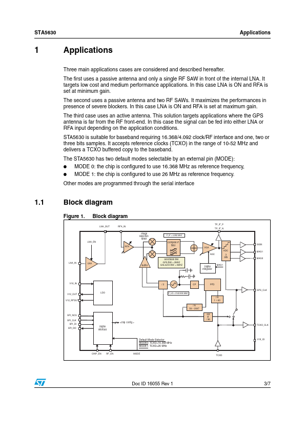
The chip is a fully integrated RF front-end able to down-convert either the GPS L1 signal from 1575.42 MHz to 4.092 MHz. A 3-bit ADC converts the IF signal to Sign (SIGN) and Magnitude (MAG0 and MAG1). The VGA gain can be also set by the SPI interface. Table 1. Device summary Marking STA5630 STA5630 Package VFQFPN32 VFQFPN32 Packing Tray Tape and reel The STA5630 accepts a range of reference clocks (10 to 52 MHz) and generates a 16.368 MHz sampling clock (GPS_CLK) for the baseband. The STA5630 embeds LDO to supply the internal core of the device facilitating requirements to external power supply. High performance low power and cost effective device, the STA5630 is the ideal solution for automotive, cellular and consumer battery powered applications.