STMicroelectronics STB180N55
This N-Channel enhancement mode MOSFET is the latest refinement of STMicroelectronic unique “Single Feature Size™“ strip-based process with less critical aligment steps and therefore a remarkable manufacturing reproducibility. The resulting transistor shows extremely high packing density for low on-resistance, rugged avalanche characteristics and low gate charge.| Part No. | STB180N55 |
|---|---|
| Datasheet | STB180N55 Download |
| Manufacturer |  STMicroelectronics |
| Description | N-CHANNEL Power MOSFET |
| Buy | Stock & Price |
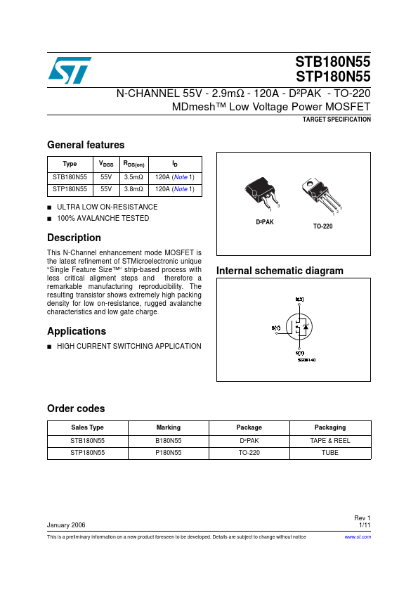
DESCRIPTION
Internal schematic diagramAPPLICATIONS
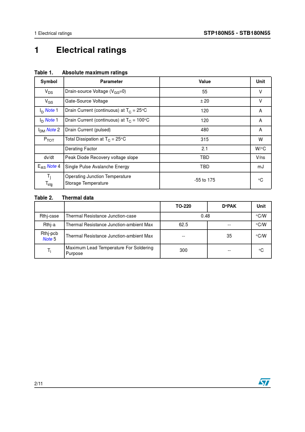
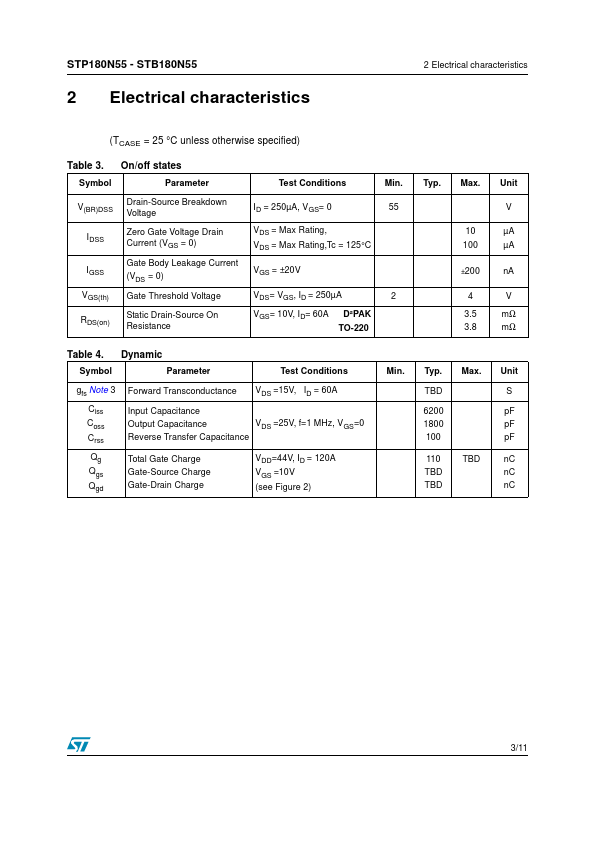
● HIGH CURRENT SWITCHING APPLICATION Order codes Sales Type STB180N55 STP180N55 Marking B180N55 P180N55 Package D²PAK TO-220 Packaging TAPE & REEL TUBE January 2006 This is a preliminary information on a new product foreseen to be developed. Details are subject to change without notice Rev 1 1/11 11 1 Electrical ratings STP180N55 - STB180N55 1 Table 1. Electrical ratings Absolute maximum ratings Parameter Drain-source Voltage (VGS=0) Gate-Source Voltage Drain Current (continuous) at TC = 25°C Drain Current (continuous) at TC = 100°C Drain Current (pulsed) Total Dissipation at TC = 25°C Derating Factor dv/dt Peak Diode Recovery voltage slope Single Pulse Avalanche Energy Operating Junction Temperature Storage Temperature Value 55 ± 20 120 120 480 315 2.1 TBD TBD -55 to 175 Unit V V A A A W W/°C V/ns mJ °C Symbol VDS VGS ID Note 1 ID Note 1 IDM Note 2 PTOT EAS Note 4 Tj Tstg Table 2. Thermal data TO-220 D²PAK 0.48 62.5 -300 -35 -Unit °C...